
| Date | 4th, Sep 2019 |
|---|
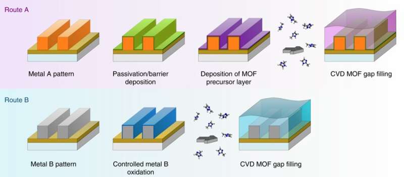
 Fig. 1From: Vapor-deposited zeolitic imidazolate frameworks as gap-filling ultra-low-k dielectrics Two proposed routes for the integration of ultra-low-k MOF dielectrics in on-chip interconnects via the MOF-CVD process. Routes A and B differ in how the MOF precursor layer is formed around the interconnect wires. In Route A, metal oxide to be converted into MOF is deposited after passivation of metal lines, while Route B relies on selective conversion of metal oxide formed through controlled oxidation of the metal pattern
Researchers at KU Leuven and imec have successfully developed a new technique to insulate microchips. The technique uses metal-organic frameworks, a new type of materials consisting of structured nanopores. In the long term, this method can be used for the development of even smaller and more powerful chips that consume less energy. The team has received an ERC Proof of Concept grant to further their research.
Computer chips are getting increasingly smaller. That's not new: Gordon Moore, one of the founders of chip manufacturer Intel, already predicted it in 1965. Moore's law states that the number of transistors in a chip, or integrated circuit, doubles about every two years. This prognosis was later adjusted to 18 months, but the theory still stands. Chips are getting smaller and their processing power is increasing. Nowadays, a chip can have over a billion transistors.
But this continued reduction in size also brings with it a number of obstacles. The switches and wires are packed together so tightly that they generate more resistance. This, in turn, causes the chip to consume more energy to send signals. To have a well-functioning chip, you need an insulating substance that separates the wires from each other, and ensures that the electrical signals are not disrupted. However, that's not an easy thing to achieve at the nanoscale level.
Nanoporous crystals
A study led by KU Leuven professor Rob Ameloot (Department of Microbial and Molecular systems) shows that a new technique might provide the solution. "We're using metal-organic frameworks (MOFs) as the insulating substance. These are materials that consist of metal ions and organic molecules. Together, they form a crystal that is porous yet sturdy."
For the first time, a research team at KU Leuven and imec managed to apply the MOF insulation to electronic material. An industrial method called chemical vapor deposition was used for this, says postdoctoral researcher Mikhail Krishtab (Department of Microbial and Molecular systems). "First, we place an oxide film on the surface. Then, we let it react with vapour of the organic material. This reaction causes the material to expand, forming the nanoporous crystals."
"The main advantage of this method is that it's bottom-up," says Krishtab. "We first deposit an oxide film, which then swells up to a very porous MOF material. You can compare it to a soufflé that puffs up in the oven and becomes very light. The MOF material forms a porous structure that fills all the gaps between the conductors. That's how we know the insulation is complete and homogeneous. With other, top-down methods, there's always still the risk of small gaps in the insulation."
Powerful and energy efficient
Professor Ameloot's research group has received an ERC Proof of Concept grant to further develop the technique, in collaboration with Silvia Armini from imec's team working on advanced dielectric materials for nanochips. "At imec, we have the expertise to develop wafer-based solutions, scaling technologies from lab to fab and paving the way to realizing a manufacturable solution for the microelectronics industry."
"We've shown that the MOF material has the right properties," Ameloot continues. "Now, we just have to refine the finishing. The surface of the crystals is still irregular at the moment. We have to smoothen this to integrate the material in a chip."
Once the technique has been perfected, it can be used to create powerful, small chips that consume less energy.
Ameloot: "Various AI applications require a lot of processing power. Think of self-driving cars and smart cities. Technology companies are constantly looking for new solutions that are both quick and energy efficient. Our research can be a valuable contribution to a new generation of chips."
More information: Mikhail Krishtab et al. Vapor-deposited zeolitic imidazolate frameworks as gap-filling ultra-low-k dielectrics, Nature Communications (2019). DOI: 10.1038/s41467-019-11703-x
Citation: New insulation technique paves the way for more powerful and smaller chips (2019, September 4) retrieved 5 July 2022 from https://phys.org/news/2019-09-insulation-technique-paves-powerful-smaller.html
This document is subject to copyright. Apart from any fair dealing for the purpose of private study or research, no part may be reproduced without the written permission. The content is provided for information purposes only.
