| Date | 14th, Sep 2019 |
|---|
Home > Press > Optical vacuum cleaner can manipulate nanoparticles: The TPU and international researchers developed a concept for constructing an optical vacuum cleaner; due to its optical properties, it can trap nanoparticles from the environment; currently, there are no sufficiently effective
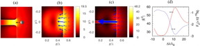 (a) Schematic diagram for the "optical vacuum cleaner", where a nanoparticle is pulled by the optical force, and moves towards the nanohole structured dielectric cuboid. (b,c) Light intensity (|E|2) and optical force distributions for (b) solid cuboid without a hole, (c) cuboid with a 20?nm hole. The refractive index and size of the simulated cuboids are set to be n?=?2 and L?=?λ. (d) Optical force and light intensity vs illumination wavelength, at the opening of the nanohole. The optical force is assumed to be exerted on a gold nanosphere with the radius of d?=?15?nm and complex dielectric permittivity εp?=??9.421?+?1.504 i at λ?=?600?nm35, and calculated using the dipole approximation. The arrows in blue color represent the optical gradient force.
CREDIT
Tomsk Polytechnic University
(a) Schematic diagram for the "optical vacuum cleaner", where a nanoparticle is pulled by the optical force, and moves towards the nanohole structured dielectric cuboid. (b,c) Light intensity (|E|2) and optical force distributions for (b) solid cuboid without a hole, (c) cuboid with a 20?nm hole. The refractive index and size of the simulated cuboids are set to be n?=?2 and L?=?λ. (d) Optical force and light intensity vs illumination wavelength, at the opening of the nanohole. The optical force is assumed to be exerted on a gold nanosphere with the radius of d?=?15?nm and complex dielectric permittivity εp?=??9.421?+?1.504 i at λ?=?600?nm35, and calculated using the dipole approximation. The arrows in blue color represent the optical gradient force.
CREDIT
Tomsk Polytechnic University
Abstract: Scientists of Tomsk Polytechnic University jointly with Russian and international colleagues developed the concept for constructing an "optical vacuum cleaner". Due to its optical properties, it can trap nanoparticles from the environment. Currently, there are no effective devices for this task. The research results were published in Scientific Reports (IF:4,525; Q1). In the future, such "vacuum cleaners" can be utilized for air purification during lab-on-a-chip operations and preparation of clean rooms.
Tomsk, Russia | Posted on September 13th, 2019
"The size of nanoparticles varies from 1 to a maximum of 100 nanometers. Currently, researchers from all around the world are seeking for the ways to control such small particles and manipulate them for various applications. However, there have been no sufficiently effective and widely used devices for such tasks yet. We offer a new concept for particle manipulation and capture - it is "optical vacuum cleaner" - says Oleg Minin, Professor of the TPU Division for Electronic Engineering.
According to this concept, an "optical vacuum cleaner" is a dielectric microparticle. In the published article, the scientists used particles having the shape of an equilateral cuboid. The particles have a nanoscale gouge or nanohole. When they are exposed to optical radiation, such as laser, there is optical pressure.
"The resultant force is directed inside our cuboid, trapping nanoparticles into the hole. The ?apacity, respectively, depends on the size of the hole", - says the scientist.
This concept can be implemented in the so-called lab-on-a-chip work in biomedical research. This technique can combine several laboratory functions on a chip, varying in size from a few square millimeters to square centimeters. This advanced on-chip analysis method will allow achieving high-throughput screening and automation. Cleaning chip surface and ambient air from foreign nanoparticles will allow increasing the analyzes sensitivity and the result accuracy.
The study was conduct by Russian and international specialists from Jilin University (China) and Ben-Gurion University (Israel). The next stage will be experimental confirmation of the concept.
####
For more information, please click here
Contacts:Vitalii Sdelnikov
7-382-260-6404
Copyright © Tomsk Polytechnic University
If you have a comment, please Contact us.
Issuers of news releases, not 7th Wave, Inc. or Nanotechnology Now, are solely responsible for the accuracy of the content.
Bookmark:


News and information
![]() Two opposing approaches could give lithium-sulfur batteries a leg up over lithium-ion July 1st, 2022
Two opposing approaches could give lithium-sulfur batteries a leg up over lithium-ion July 1st, 2022
![]() Efficiently processing high-quality periodic nanostructures with ultrafast laser July 1st, 2022
Efficiently processing high-quality periodic nanostructures with ultrafast laser July 1st, 2022
![]() Photonic synapses with low power consumption and high sensitivity are expected to integrate sensing-memory-preprocessing capabilities July 1st, 2022
Photonic synapses with low power consumption and high sensitivity are expected to integrate sensing-memory-preprocessing capabilities July 1st, 2022
Lab-on-a-chip
![]() Micro-scale opto-thermo-mechanical actuation in the dry adhesive regime Peer-Reviewed Publication September 24th, 2021
Micro-scale opto-thermo-mechanical actuation in the dry adhesive regime Peer-Reviewed Publication September 24th, 2021
![]() Silicon-graphene hybrid plasmonic waveguide photodetectors beyond 1.55 μm March 13th, 2020
Silicon-graphene hybrid plasmonic waveguide photodetectors beyond 1.55 μm March 13th, 2020
Possible Futures
![]() Sieving carbons: Ideal anodes for high-energy sodium-ion batteries July 1st, 2022
Sieving carbons: Ideal anodes for high-energy sodium-ion batteries July 1st, 2022
![]() An artificial intelligence probe help see tumor malignancy July 1st, 2022
An artificial intelligence probe help see tumor malignancy July 1st, 2022
![]() Photon-controlled diode: an optoelectronic device with a new signal processing behavior July 1st, 2022
Photon-controlled diode: an optoelectronic device with a new signal processing behavior July 1st, 2022
Chip Technology
![]() Photon-controlled diode: an optoelectronic device with a new signal processing behavior July 1st, 2022
Photon-controlled diode: an optoelectronic device with a new signal processing behavior July 1st, 2022
![]() Photonic synapses with low power consumption and high sensitivity are expected to integrate sensing-memory-preprocessing capabilities July 1st, 2022
Photonic synapses with low power consumption and high sensitivity are expected to integrate sensing-memory-preprocessing capabilities July 1st, 2022
Nanoelectronics
![]() Controlled synthesis of crystal flakes paves path for advanced future electronics June 17th, 2022
Controlled synthesis of crystal flakes paves path for advanced future electronics June 17th, 2022
![]() Eyebrow-raising: Researchers reveal why nanowires stick to each other February 11th, 2022
Eyebrow-raising: Researchers reveal why nanowires stick to each other February 11th, 2022
![]() Visualizing temperature transport: An unexpected technique for nanoscale characterization November 19th, 2021
Visualizing temperature transport: An unexpected technique for nanoscale characterization November 19th, 2021
Discoveries
![]() Sieving carbons: Ideal anodes for high-energy sodium-ion batteries July 1st, 2022
Sieving carbons: Ideal anodes for high-energy sodium-ion batteries July 1st, 2022
![]() Efficiently processing high-quality periodic nanostructures with ultrafast laser July 1st, 2022
Efficiently processing high-quality periodic nanostructures with ultrafast laser July 1st, 2022
![]() Photonic synapses with low power consumption and high sensitivity are expected to integrate sensing-memory-preprocessing capabilities July 1st, 2022
Photonic synapses with low power consumption and high sensitivity are expected to integrate sensing-memory-preprocessing capabilities July 1st, 2022
Announcements
![]() Two opposing approaches could give lithium-sulfur batteries a leg up over lithium-ion July 1st, 2022
Two opposing approaches could give lithium-sulfur batteries a leg up over lithium-ion July 1st, 2022
![]() Efficiently processing high-quality periodic nanostructures with ultrafast laser July 1st, 2022
Efficiently processing high-quality periodic nanostructures with ultrafast laser July 1st, 2022
![]() Photonic synapses with low power consumption and high sensitivity are expected to integrate sensing-memory-preprocessing capabilities July 1st, 2022
Photonic synapses with low power consumption and high sensitivity are expected to integrate sensing-memory-preprocessing capabilities July 1st, 2022
Interviews/Book Reviews/Essays/Reports/Podcasts/Journals/White papers/Posters
![]() Sieving carbons: Ideal anodes for high-energy sodium-ion batteries July 1st, 2022
Sieving carbons: Ideal anodes for high-energy sodium-ion batteries July 1st, 2022
![]() An artificial intelligence probe help see tumor malignancy July 1st, 2022
An artificial intelligence probe help see tumor malignancy July 1st, 2022
![]() Photon-controlled diode: an optoelectronic device with a new signal processing behavior July 1st, 2022
Photon-controlled diode: an optoelectronic device with a new signal processing behavior July 1st, 2022
Tools
![]() New technology helps reveal inner workings of human genome June 24th, 2022
New technology helps reveal inner workings of human genome June 24th, 2022
![]() Snapshot measurement of single nanostructure�s circular dichroism March 25th, 2022
Snapshot measurement of single nanostructure�s circular dichroism March 25th, 2022
![]() Eyebrow-raising: Researchers reveal why nanowires stick to each other February 11th, 2022
Eyebrow-raising: Researchers reveal why nanowires stick to each other February 11th, 2022
![]() JEOL Introduces New Scanning Electron Microscope with �Simple SEM� Automation and Live Elemental and 3D Analysis January 14th, 2022
JEOL Introduces New Scanning Electron Microscope with �Simple SEM� Automation and Live Elemental and 3D Analysis January 14th, 2022
Photonics/Optics/Lasers
![]() Photon-controlled diode: an optoelectronic device with a new signal processing behavior July 1st, 2022
Photon-controlled diode: an optoelectronic device with a new signal processing behavior July 1st, 2022
![]() Efficiently processing high-quality periodic nanostructures with ultrafast laser July 1st, 2022
Efficiently processing high-quality periodic nanostructures with ultrafast laser July 1st, 2022
![]() Photonic synapses with low power consumption and high sensitivity are expected to integrate sensing-memory-preprocessing capabilities July 1st, 2022
Photonic synapses with low power consumption and high sensitivity are expected to integrate sensing-memory-preprocessing capabilities July 1st, 2022
