| Date | 7th, Mar 2020 |
|---|
Home > Press > Comprehensive review of heterogeneously integrated 2D materials
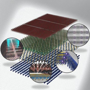 Schematic illustration of the newly emerged 2D heterostructures research with various heterogeneous integration of 2D materials.
CREDIT
Author
Schematic illustration of the newly emerged 2D heterostructures research with various heterogeneous integration of 2D materials.
CREDIT
Author
Abstract: In a paper published in NANO, a group of researchers from Sungkyunkwan University, South Korea provide a comprehensive review of heterogeneously integrated two dimensional (2D) materials from an extensive library of atomic 2D materials with selectable material properties to open up fascinating possibilities for the design of functional novel devices.
Singapore | Posted on March 6th, 2020
Since the discovery of Graphene by Andre Geim and Konstantin Novoselov, 2D materials, e.g., graphene, black phosphorous (BP), transition metal dichalcogenides (TMDCs), and hexagonal boron nitride (h-BN) have attracted extensive attention due to their broad physical properties and wide range of applications to electronic and optoelectronic devices. Research on these 2D materials has matured to the point where an extensive library of atomically thin 2D materials with selectable material properties has been created and continues to grow.
By combining or stacking these 2D materials, it is possible to construct 2D heterostructures, which are built by directly stacking individual monolayers comprising different materials. Each monolayer within a 2D heterostructure is highly stable, due to strong covalent bonds between the atoms within that monolayer. However, the forces between the monolayers that keep said monolayers stacked one above the other to form the 2D heterostructure happen to be relatively weak van der Waals interactions. Due to this, each of the monolayers retains its intrinsic properties. Moreover, unlike in conventional semiconductor heterostructures where component material selection is restricted to those with similar lattice structures, the lattice mismatch requirements of stacked heterostructures can be relaxed due to the weakness of the van der Waal's forces. This means that one can combine insulating, semiconducting, or metallic 2D materials to form a single 2D heterostructure despite their different lattice structures.
When a monolayer is stacked in combination with other monolayers made out of different materials, a variety of new heterostructures with atomically thin 2D heterojunctions can be created. Heterostructures made from a particular combination of materials will have a certain set of physical characteristics depending on which materials they are made from. The unusual physical characteristics of 2D heterostructures make them suitable for use in a wide range of applications.
In this review, various 2D heterostructures are discussed along with an explanation of novel electronic and optoelectronic properties, advanced synthesis technical developments, as well as new functional applications available. It provides an understanding of the current research trends in 2D materials, so as to explore future possibilities for nanomaterial research.
###
This research was supported by the National Research Foundation of Korea funded by the Korean government (grant nos. 2013M3A6B1078873, 2015R1D1A1A09057297, 2017R1A4A1015400, and 2017R1A2A2A05001403).
Corresponding authors for this study are Euyheon Hwang ( and Sungjoo Lee ) from SKKU Advanced Institute of Nanotechnology and Department of Nano Engineering, Sungkyunkwan University.
For more insight into the research described, readers are invited to access the paper on NANO.
####
About World ScientificWorld Scientific Publishing is a leading independent publisher of books and journals for the scholarly, research, professional and educational communities. The company publishes about 600 books annually and about 140 journals in various fields. World Scientific collaborates with prestigious organizations like the Nobel Foundation and US National Academies Press to bring high quality academic and professional content to researchers and academics worldwide. To find out more about World Scientific, please visit http://www.worldscientific.com .
For more information, please click here
Contacts:Tay Yu Shan
@worldscientific
Copyright © World Scientific
If you have a comment, please Contact us.
Issuers of news releases, not 7th Wave, Inc. or Nanotechnology Now, are solely responsible for the accuracy of the content.
Bookmark:


News and information
![]() Two opposing approaches could give lithium-sulfur batteries a leg up over lithium-ion July 1st, 2022
Two opposing approaches could give lithium-sulfur batteries a leg up over lithium-ion July 1st, 2022
![]() Efficiently processing high-quality periodic nanostructures with ultrafast laser July 1st, 2022
Efficiently processing high-quality periodic nanostructures with ultrafast laser July 1st, 2022
![]() Photonic synapses with low power consumption and high sensitivity are expected to integrate sensing-memory-preprocessing capabilities July 1st, 2022
Photonic synapses with low power consumption and high sensitivity are expected to integrate sensing-memory-preprocessing capabilities July 1st, 2022
2 Dimensional Materials
![]() Controlled synthesis of crystal flakes paves path for advanced future electronics June 17th, 2022
Controlled synthesis of crystal flakes paves path for advanced future electronics June 17th, 2022
![]() Solving the puzzle of 2D disorder: An interdisciplinary team developed a new method to characterize disorder in 2D materials June 17th, 2022
Solving the puzzle of 2D disorder: An interdisciplinary team developed a new method to characterize disorder in 2D materials June 17th, 2022
![]() UBCO researchers change the game when it comes to activity tracking: Flexible, highly sensitive motion device created by extrusion printing June 17th, 2022
UBCO researchers change the game when it comes to activity tracking: Flexible, highly sensitive motion device created by extrusion printing June 17th, 2022
![]() Bumps could smooth quantum investigations: Rice University models show unique properties of 2D materials stressed by contoured substrates June 10th, 2022
Bumps could smooth quantum investigations: Rice University models show unique properties of 2D materials stressed by contoured substrates June 10th, 2022
Graphene/ Graphite
![]() OCSiAl expands its graphene nanotube production capacities to Europe June 17th, 2022
OCSiAl expands its graphene nanotube production capacities to Europe June 17th, 2022
![]() Bumps could smooth quantum investigations: Rice University models show unique properties of 2D materials stressed by contoured substrates June 10th, 2022
Bumps could smooth quantum investigations: Rice University models show unique properties of 2D materials stressed by contoured substrates June 10th, 2022
![]() Nanotubes: a promising solution for advanced rubber cables with 60% less conductive filler June 1st, 2022
Nanotubes: a promising solution for advanced rubber cables with 60% less conductive filler June 1st, 2022
Possible Futures
![]() Sieving carbons: Ideal anodes for high-energy sodium-ion batteries July 1st, 2022
Sieving carbons: Ideal anodes for high-energy sodium-ion batteries July 1st, 2022
![]() An artificial intelligence probe help see tumor malignancy July 1st, 2022
An artificial intelligence probe help see tumor malignancy July 1st, 2022
![]() Photon-controlled diode: an optoelectronic device with a new signal processing behavior July 1st, 2022
Photon-controlled diode: an optoelectronic device with a new signal processing behavior July 1st, 2022
Discoveries
![]() Sieving carbons: Ideal anodes for high-energy sodium-ion batteries July 1st, 2022
Sieving carbons: Ideal anodes for high-energy sodium-ion batteries July 1st, 2022
![]() Efficiently processing high-quality periodic nanostructures with ultrafast laser July 1st, 2022
Efficiently processing high-quality periodic nanostructures with ultrafast laser July 1st, 2022
![]() Photonic synapses with low power consumption and high sensitivity are expected to integrate sensing-memory-preprocessing capabilities July 1st, 2022
Photonic synapses with low power consumption and high sensitivity are expected to integrate sensing-memory-preprocessing capabilities July 1st, 2022
Materials/Metamaterials
![]() New protocol for assessing the safety of nanomaterials July 1st, 2022
New protocol for assessing the safety of nanomaterials July 1st, 2022
![]() Nanotubes: a promising solution for advanced rubber cables with 60% less conductive filler June 1st, 2022
Nanotubes: a promising solution for advanced rubber cables with 60% less conductive filler June 1st, 2022
![]() New route to build materials out of tiny particles May 27th, 2022
New route to build materials out of tiny particles May 27th, 2022
![]() A one-stop shop for quantum sensing materials May 27th, 2022
A one-stop shop for quantum sensing materials May 27th, 2022
Announcements
![]() Two opposing approaches could give lithium-sulfur batteries a leg up over lithium-ion July 1st, 2022
Two opposing approaches could give lithium-sulfur batteries a leg up over lithium-ion July 1st, 2022
![]() Efficiently processing high-quality periodic nanostructures with ultrafast laser July 1st, 2022
Efficiently processing high-quality periodic nanostructures with ultrafast laser July 1st, 2022
![]() Photonic synapses with low power consumption and high sensitivity are expected to integrate sensing-memory-preprocessing capabilities July 1st, 2022
Photonic synapses with low power consumption and high sensitivity are expected to integrate sensing-memory-preprocessing capabilities July 1st, 2022
Interviews/Book Reviews/Essays/Reports/Podcasts/Journals/White papers/Posters
![]() Sieving carbons: Ideal anodes for high-energy sodium-ion batteries July 1st, 2022
Sieving carbons: Ideal anodes for high-energy sodium-ion batteries July 1st, 2022
![]() An artificial intelligence probe help see tumor malignancy July 1st, 2022
An artificial intelligence probe help see tumor malignancy July 1st, 2022
![]() Photon-controlled diode: an optoelectronic device with a new signal processing behavior July 1st, 2022
Photon-controlled diode: an optoelectronic device with a new signal processing behavior July 1st, 2022
