| Date | 14th, Mar 2020 |
|---|
Home > Press > Silicon-graphene hybrid plasmonic waveguide photodetectors beyond 1.55 μm
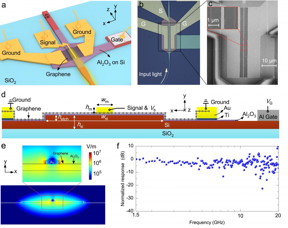 a. Schematic configuration; b. Optical microscope; c. SEM pictures; d. Cross-section of the present silicon-graphene hybrid plasmonic waveguide with the signal electrode at the middle and the ground electrodes at both sides (here the metal-graphene-metal sandwich structure is utilized); e. The electric field component distribution of the quasi-TE0 mode for the optimized silicon-graphene hybrid plasmonic waveguide; f. Measured frequency response of Device B operating at ��=2μm (bias voltage: -0.5 V, gate voltage: 2.9 V).
CREDIT
Jingshu Guo, Jiang Li, Chaoyue Liu, Yanlong Yin, Wenhui Wang, Zhenhua Ni, Zhilei Fu, Hui Yu, Yang Xu, Yaocheng Shi, Yungui Ma, Shiming Gao, Liming Tong and Daoxin Dai
a. Schematic configuration; b. Optical microscope; c. SEM pictures; d. Cross-section of the present silicon-graphene hybrid plasmonic waveguide with the signal electrode at the middle and the ground electrodes at both sides (here the metal-graphene-metal sandwich structure is utilized); e. The electric field component distribution of the quasi-TE0 mode for the optimized silicon-graphene hybrid plasmonic waveguide; f. Measured frequency response of Device B operating at ��=2μm (bias voltage: -0.5 V, gate voltage: 2.9 V).
CREDIT
Jingshu Guo, Jiang Li, Chaoyue Liu, Yanlong Yin, Wenhui Wang, Zhenhua Ni, Zhilei Fu, Hui Yu, Yang Xu, Yaocheng Shi, Yungui Ma, Shiming Gao, Liming Tong and Daoxin Dai
Abstract: Silicon photonics is known as a key technology for modern optical communications at the near infrared wavelength-band, i.e., 1.31/1.55 μm. Currently silicon photonics has been desired to be extended to the wavelength-band beyond 1.55 μm, e.g., 2 μm, for important applications in optical communications, nonlinear photonics, and on-chip sensing. However, the realization of high-performance silicon-based waveguide photodetectors beyond 1.55 μm still faces challenges since there are some fabrication issues as well as wavelength-band limitations. As an alternative, two-dimensional materials (e.g., graphene) provide a promising solution because of the ability for broad operation wavelength-bands and the advantage of avoiding structure mismatch in the design and fabrication.
Changchun, China | Posted on March 13th, 2020
In the paper published in Light: Science & Applications, scientists from Zhejiang University and Southeast University in China proposed and demonstrated high-performance waveguide photodetectors beyond 1.55 μm by introducing a novel silicon-graphene hybrid plasmonic waveguide. In particular, an ultra-thin wide silicon ridge core region with a metal cap atop is introduced to obtain a unique mode field profile, so that light absorption of graphene is enhanced. Furthermore, the fabrication is easy and the graphene-metal contact resistance is reduced, compared to the previous silicon-graphene hybrid waveguides. For example, the graphene absorption efficiencies are as high as 54.3% and 68.6% for 20 μm-long and 50 μm-long absorption regions, when operating at 1.55 μm and 2 μm, respectively.
For the fabricated photodetectors operating at 2 μm, the measured 3 dB-bandwidths are >20 GHz (limited by the experimental setup), while the responsivities are 30-70 mA/W for 0.28 mW input optical power under -0.3V bias voltage. For the photodetectors operating at 1.55 μm, the 3 dB-bandwidth is >40 GHz (limited by the setup), while the measured responsivity is about 0.4 A/W for 0.16 mW input optical power under -0.3V bias voltage.
In this work, the mechanisms in graphene photodetectors are analyzed carefully, which suggested that the photo-thermoelectric effect is the dominant mechanism for photo-response when operating at zero bias voltage. When the photodetector operates at non-zero bias voltages, the dominant mechanism becomes the bolometric or photoconductive effect. This comprehensive analysis helps better understand the photocurrent generation in the graphene-metal interfaces.
These scientists summarize the highlights of their work:
"We have proposed and demonstrated high-performance silicon-graphene hybrid plasmonic waveguide photodetectors beyond 1.55 μm. In particular, a novel silicon-graphene hybrid plasmonic waveguide was used by introducing an ultra-thin wide silicon ridge core region with a metal cap atop. The optical modal filed is manipulated in both vertical and horizontal directions. Thus, the light absorption in graphene is enhanced, meanwhile the metal absorption loss is minimized. This greatly helps achieve sufficient light absorption of graphene within a short absorption region."
"The silicon-graphene waveguide photodetectors operating at 2 μm were demonstrated with a 3 dB-bandwidth over 20 GHz. The measured responsivity is 30-70 mA/W at the bias voltage of -0.3V for input optical power of 0.28 mW. The photodetector at 1.55 μm was also demonstrated with excellent performances. The present work paves the way for achieving high-responsivity and high-speed waveguide photodetectors on silicon for near/mid-infrared wavelength-bands" they added.
"In future works, more efforts should be given to introduce some special junction structures to minimize the dark current and further extend the operation wavelength-band. Graphene waveguide photodetectors may play an important role in mid-infrared silicon photonics, which will play an important role in time resolved spectroscopy, lab-on-chip sensing, nonlinear photonics, as well as optical communication" they said.
####
For more information, please click here
Contacts:Daoxin Dai
Copyright © Changchun Institute of Optics, Fine Mechanics and Physics, Chinese Academy of Sciences
If you have a comment, please Contact us.
Issuers of news releases, not 7th Wave, Inc. or Nanotechnology Now, are solely responsible for the accuracy of the content.
Bookmark:


Imaging
![]() An artificial intelligence probe help see tumor malignancy July 1st, 2022
An artificial intelligence probe help see tumor malignancy July 1st, 2022
News and information
![]() Two opposing approaches could give lithium-sulfur batteries a leg up over lithium-ion July 1st, 2022
Two opposing approaches could give lithium-sulfur batteries a leg up over lithium-ion July 1st, 2022
![]() Efficiently processing high-quality periodic nanostructures with ultrafast laser July 1st, 2022
Efficiently processing high-quality periodic nanostructures with ultrafast laser July 1st, 2022
![]() Photonic synapses with low power consumption and high sensitivity are expected to integrate sensing-memory-preprocessing capabilities July 1st, 2022
Photonic synapses with low power consumption and high sensitivity are expected to integrate sensing-memory-preprocessing capabilities July 1st, 2022
Wireless/telecommunications/RF/Antennas/Microwaves
![]() Quantum network nodes with warm atoms June 24th, 2022
Quantum network nodes with warm atoms June 24th, 2022
![]() Photonic integrated erbium doped amplifiers reach commercial performance: Boosting light power revolutionizes communications and autopilots June 17th, 2022
Photonic integrated erbium doped amplifiers reach commercial performance: Boosting light power revolutionizes communications and autopilots June 17th, 2022
![]() Nanoscale bowtie antenna under optical and electrical excitations June 3rd, 2022
Nanoscale bowtie antenna under optical and electrical excitations June 3rd, 2022
Graphene/ Graphite
![]() OCSiAl expands its graphene nanotube production capacities to Europe June 17th, 2022
OCSiAl expands its graphene nanotube production capacities to Europe June 17th, 2022
![]() Bumps could smooth quantum investigations: Rice University models show unique properties of 2D materials stressed by contoured substrates June 10th, 2022
Bumps could smooth quantum investigations: Rice University models show unique properties of 2D materials stressed by contoured substrates June 10th, 2022
Lab-on-a-chip
![]() Micro-scale opto-thermo-mechanical actuation in the dry adhesive regime Peer-Reviewed Publication September 24th, 2021
Micro-scale opto-thermo-mechanical actuation in the dry adhesive regime Peer-Reviewed Publication September 24th, 2021
![]() Trapping and moving tiny particles using light September 24th, 2019
Trapping and moving tiny particles using light September 24th, 2019
Govt.-Legislation/Regulation/Funding/Policy
![]() Solving the solar energy storage problem with rechargeable batteries that can convert and store energy at once June 24th, 2022
Solving the solar energy storage problem with rechargeable batteries that can convert and store energy at once June 24th, 2022
![]() Boron nitride nanotube fibers get real: Rice lab creates first heat-tolerant, stable fibers from wet-spinning process June 24th, 2022
Boron nitride nanotube fibers get real: Rice lab creates first heat-tolerant, stable fibers from wet-spinning process June 24th, 2022
![]() UBCO researchers change the game when it comes to activity tracking: Flexible, highly sensitive motion device created by extrusion printing June 17th, 2022
UBCO researchers change the game when it comes to activity tracking: Flexible, highly sensitive motion device created by extrusion printing June 17th, 2022
![]() University of Illinois Chicago joins Brookhaven Lab's Quantum Center June 10th, 2022
University of Illinois Chicago joins Brookhaven Lab's Quantum Center June 10th, 2022
Possible Futures
![]() Sieving carbons: Ideal anodes for high-energy sodium-ion batteries July 1st, 2022
Sieving carbons: Ideal anodes for high-energy sodium-ion batteries July 1st, 2022
![]() An artificial intelligence probe help see tumor malignancy July 1st, 2022
An artificial intelligence probe help see tumor malignancy July 1st, 2022
![]() Photon-controlled diode: an optoelectronic device with a new signal processing behavior July 1st, 2022
Photon-controlled diode: an optoelectronic device with a new signal processing behavior July 1st, 2022
Discoveries
![]() Sieving carbons: Ideal anodes for high-energy sodium-ion batteries July 1st, 2022
Sieving carbons: Ideal anodes for high-energy sodium-ion batteries July 1st, 2022
![]() Efficiently processing high-quality periodic nanostructures with ultrafast laser July 1st, 2022
Efficiently processing high-quality periodic nanostructures with ultrafast laser July 1st, 2022
![]() Photonic synapses with low power consumption and high sensitivity are expected to integrate sensing-memory-preprocessing capabilities July 1st, 2022
Photonic synapses with low power consumption and high sensitivity are expected to integrate sensing-memory-preprocessing capabilities July 1st, 2022
Announcements
![]() Two opposing approaches could give lithium-sulfur batteries a leg up over lithium-ion July 1st, 2022
Two opposing approaches could give lithium-sulfur batteries a leg up over lithium-ion July 1st, 2022
![]() Efficiently processing high-quality periodic nanostructures with ultrafast laser July 1st, 2022
Efficiently processing high-quality periodic nanostructures with ultrafast laser July 1st, 2022
![]() Photonic synapses with low power consumption and high sensitivity are expected to integrate sensing-memory-preprocessing capabilities July 1st, 2022
Photonic synapses with low power consumption and high sensitivity are expected to integrate sensing-memory-preprocessing capabilities July 1st, 2022
Interviews/Book Reviews/Essays/Reports/Podcasts/Journals/White papers/Posters
![]() Sieving carbons: Ideal anodes for high-energy sodium-ion batteries July 1st, 2022
Sieving carbons: Ideal anodes for high-energy sodium-ion batteries July 1st, 2022
![]() An artificial intelligence probe help see tumor malignancy July 1st, 2022
An artificial intelligence probe help see tumor malignancy July 1st, 2022
![]() Photon-controlled diode: an optoelectronic device with a new signal processing behavior July 1st, 2022
Photon-controlled diode: an optoelectronic device with a new signal processing behavior July 1st, 2022
Photonics/Optics/Lasers
![]() Photon-controlled diode: an optoelectronic device with a new signal processing behavior July 1st, 2022
Photon-controlled diode: an optoelectronic device with a new signal processing behavior July 1st, 2022
![]() Efficiently processing high-quality periodic nanostructures with ultrafast laser July 1st, 2022
Efficiently processing high-quality periodic nanostructures with ultrafast laser July 1st, 2022
![]() Photonic synapses with low power consumption and high sensitivity are expected to integrate sensing-memory-preprocessing capabilities July 1st, 2022
Photonic synapses with low power consumption and high sensitivity are expected to integrate sensing-memory-preprocessing capabilities July 1st, 2022
Research partnerships
![]() New technology helps reveal inner workings of human genome June 24th, 2022
New technology helps reveal inner workings of human genome June 24th, 2022
![]() Boron nitride nanotube fibers get real: Rice lab creates first heat-tolerant, stable fibers from wet-spinning process June 24th, 2022
Boron nitride nanotube fibers get real: Rice lab creates first heat-tolerant, stable fibers from wet-spinning process June 24th, 2022
