| Date | 21st, Mar 2020 |
|---|
Home > Press > O-FIB: Far-field-induced near-field breakdown for direct nanowriting in an atmospheric environment
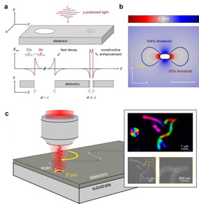 a, Schematic plot of the evanescent wave (Eew) around two nanoholes with different sizes on a dielectric. For the larger nanohole with a diameter comparable to the wavelength, the evanescent fields at each edge of the nanohole are independent and decay rapidly from the boundary. For the smaller nanohole with a deep-subwavelength aperture, the strong interaction between the two boundaries constructively enhances the optical intensity inside the nanohole and confines the light on a deep-subwavelength scale. b, Simulations of the E-field strength distribution for a titanium oxide film with a nanohole shown by the central white-out region (the intensity of the light inside the nanohole is close to maximum but is not shown for a better visualization). c, Schematic of the direct nanowriting of O-FIB (left) and the image of the free-form patterning obtained by birefringence microscope (right, upper) and scanning electron microscope (right, lower).
CREDIT
by Zhen-Ze Li, Lei Wang, Hua Fan, Yan-Hao Yu, Qi-Dai Chen, Saulius Juodkazis and Hong-Bo Sun
a, Schematic plot of the evanescent wave (Eew) around two nanoholes with different sizes on a dielectric. For the larger nanohole with a diameter comparable to the wavelength, the evanescent fields at each edge of the nanohole are independent and decay rapidly from the boundary. For the smaller nanohole with a deep-subwavelength aperture, the strong interaction between the two boundaries constructively enhances the optical intensity inside the nanohole and confines the light on a deep-subwavelength scale. b, Simulations of the E-field strength distribution for a titanium oxide film with a nanohole shown by the central white-out region (the intensity of the light inside the nanohole is close to maximum but is not shown for a better visualization). c, Schematic of the direct nanowriting of O-FIB (left) and the image of the free-form patterning obtained by birefringence microscope (right, upper) and scanning electron microscope (right, lower).
CREDIT
by Zhen-Ze Li, Lei Wang, Hua Fan, Yan-Hao Yu, Qi-Dai Chen, Saulius Juodkazis and Hong-Bo Sun
Abstract: Lasers are becoming one of the dominant tools in the current manufacturing industry. Much effort has been devoted to improving the processing accuracy, and spatial resolutions as low as micrometers have been achieved in laser cutting, wedding, marking and stereolithography in an atmospheric environment. The femtosecond laser (fs-laser) is a particularly promising approach from this point of view, in addition to its three-dimensional (3D) processing capability and broad-spectrum material usability. Super-diffraction-limited feature sizes at a level of tens of nanometers based on multiphoton absorption thresholding, shrinkage and stimulation emission depletion effects have also been realized in fs-laser induced photocuring of polymers, which unfortunately are not applicable to solid materials. Optical near-field techniques provide an alternative super-resolution scheme by localizing light fields to nanometer scales with the physical shapes of sharp tips, tiny apertures, nanoparticles and small protrusions. Nevertheless, these approaches often rely on heavy movement and alignment systems to maintain precise probe-substrate spacing for practical fabrication/patterning throughput due to the evanescent nature of the near field. An innovative optical patterning technology that permits vacuum-free high-resolution processing comparable to conventional FIB processing is highly desired.In a new paper published in Light Science & Application, scientists from the State Key Laboratory of Precision Measurement Technology and Instruments, Department of Precision Instrument, Tsinghua University, Beijing, China, the State Key Laboratory of Integrated Optoelectronics, College of Electronic Science and Engineering, Jilin University, Changchun, China, and the Nanotechnology facility, Swinburne University of Technology, John st., Hawthorn, Australia reported an optical far-field-induced near-field breakdown (O-FIB) approach, allowing the nanofabrication applicable to almost any solid materials in atmosphere. The writing is initiated from nano-holes created by femtosecond laser induced multiphoton absorption and its cutting "knife edge" is sharpened by far-field regulated enhancement of the optical near field. A spatial resolution of sub-20 nm (λ/40 for light wavelength λ) is readily achieved. O-FIB is empowered by a simple polarization control of the incident light for steering nano-groove writing along the designed pattern.
Changchun, China | Posted on March 20th, 2020
"According to the continuous boundary condition of the normal component of electric displacement, we experimentally observed the light field nano-localization and polarization-vertical enhancement around the nanohole, which permits direct control of the near-field enhancement for nanoablation by far field. Based on this idea, we have realized free nano-writing with resolution as high as 18 nm by manipulating laser polarization and beam's trajectory in real time."
"Since for the self-regulation effect induced by the feedback between light and the initial seeds, our approach has the inherent robustness against the stochastic nature of initial ablation and the ability to manipulate line width. Besides, our approach demonstrates free-form stitchless writing of nano-grooves with controllable length, separation and trajectory. Meanwhile, the universality of seeding effect enables a large-area printing mode which is superior to the conventional FIB."
"Our presented technique has opened a new era of high-efficient nanomachining. It is applicable for various materials and surface in the fields of nanoelectronics, nanofluids, and nanomedicines. The possibility we show here to direct manipulating the near field through the far field, may inspire the researchers to push the femtosecond laser nanofabrication or even other domains of the optical processing to a higher level." The scientists forecast.
####
For more information, please click here
Contacts:Hong-Bo Sun
Copyright © Changchun Institute of Optics, Fine Mechanics and Physics, Chinese Academy of Sciences
If you have a comment, please Contact us.
Issuers of news releases, not 7th Wave, Inc. or Nanotechnology Now, are solely responsible for the accuracy of the content.
Bookmark:


Microfluidics/Nanofluidics
![]() Oregon State University research pushes closer to new therapy for pancreatic cancer May 6th, 2022
Oregon State University research pushes closer to new therapy for pancreatic cancer May 6th, 2022
Nanofabrication
![]() First integrated laser on lithium niobate chip: Research paves the way for high-powered telecommunication systems April 8th, 2022
First integrated laser on lithium niobate chip: Research paves the way for high-powered telecommunication systems April 8th, 2022
![]() Atom by atom: building precise smaller nanoparticles with templates March 4th, 2022
Atom by atom: building precise smaller nanoparticles with templates March 4th, 2022
![]() Review on the femtosecond laser precision micro/nano-engineering December 3rd, 2021
Review on the femtosecond laser precision micro/nano-engineering December 3rd, 2021
Govt.-Legislation/Regulation/Funding/Policy
![]() Solving the solar energy storage problem with rechargeable batteries that can convert and store energy at once June 24th, 2022
Solving the solar energy storage problem with rechargeable batteries that can convert and store energy at once June 24th, 2022
![]() Boron nitride nanotube fibers get real: Rice lab creates first heat-tolerant, stable fibers from wet-spinning process June 24th, 2022
Boron nitride nanotube fibers get real: Rice lab creates first heat-tolerant, stable fibers from wet-spinning process June 24th, 2022
![]() UBCO researchers change the game when it comes to activity tracking: Flexible, highly sensitive motion device created by extrusion printing June 17th, 2022
UBCO researchers change the game when it comes to activity tracking: Flexible, highly sensitive motion device created by extrusion printing June 17th, 2022
![]() University of Illinois Chicago joins Brookhaven Lab's Quantum Center June 10th, 2022
University of Illinois Chicago joins Brookhaven Lab's Quantum Center June 10th, 2022
Possible Futures
![]() New technology helps reveal inner workings of human genome June 24th, 2022
New technology helps reveal inner workings of human genome June 24th, 2022
![]() Boron nitride nanotube fibers get real: Rice lab creates first heat-tolerant, stable fibers from wet-spinning process June 24th, 2022
Boron nitride nanotube fibers get real: Rice lab creates first heat-tolerant, stable fibers from wet-spinning process June 24th, 2022
Nanomedicine
![]() New technology helps reveal inner workings of human genome June 24th, 2022
New technology helps reveal inner workings of human genome June 24th, 2022
![]() New nano-gel to protect children receiving chemotherapy from hearing loss June 17th, 2022
New nano-gel to protect children receiving chemotherapy from hearing loss June 17th, 2022
Nanoelectronics
![]() Controlled synthesis of crystal flakes paves path for advanced future electronics June 17th, 2022
Controlled synthesis of crystal flakes paves path for advanced future electronics June 17th, 2022
![]() Eyebrow-raising: Researchers reveal why nanowires stick to each other February 11th, 2022
Eyebrow-raising: Researchers reveal why nanowires stick to each other February 11th, 2022
![]() Visualizing temperature transport: An unexpected technique for nanoscale characterization November 19th, 2021
Visualizing temperature transport: An unexpected technique for nanoscale characterization November 19th, 2021
Discoveries
![]() New technology helps reveal inner workings of human genome June 24th, 2022
New technology helps reveal inner workings of human genome June 24th, 2022
![]() Boron nitride nanotube fibers get real: Rice lab creates first heat-tolerant, stable fibers from wet-spinning process June 24th, 2022
Boron nitride nanotube fibers get real: Rice lab creates first heat-tolerant, stable fibers from wet-spinning process June 24th, 2022
Announcements
![]() New technology helps reveal inner workings of human genome June 24th, 2022
New technology helps reveal inner workings of human genome June 24th, 2022
![]() Boron nitride nanotube fibers get real: Rice lab creates first heat-tolerant, stable fibers from wet-spinning process June 24th, 2022
Boron nitride nanotube fibers get real: Rice lab creates first heat-tolerant, stable fibers from wet-spinning process June 24th, 2022
Interviews/Book Reviews/Essays/Reports/Podcasts/Journals/White papers/Posters
![]() Quantum network nodes with warm atoms June 24th, 2022
Quantum network nodes with warm atoms June 24th, 2022
![]() New technology helps reveal inner workings of human genome June 24th, 2022
New technology helps reveal inner workings of human genome June 24th, 2022
Grants/Sponsored Research/Awards/Scholarships/Gifts/Contests/Honors/Records
![]() Solving the solar energy storage problem with rechargeable batteries that can convert and store energy at once June 24th, 2022
Solving the solar energy storage problem with rechargeable batteries that can convert and store energy at once June 24th, 2022
![]() Boron nitride nanotube fibers get real: Rice lab creates first heat-tolerant, stable fibers from wet-spinning process June 24th, 2022
Boron nitride nanotube fibers get real: Rice lab creates first heat-tolerant, stable fibers from wet-spinning process June 24th, 2022
Photonics/Optics/Lasers
![]() Photonic integrated erbium doped amplifiers reach commercial performance: Boosting light power revolutionizes communications and autopilots June 17th, 2022
Photonic integrated erbium doped amplifiers reach commercial performance: Boosting light power revolutionizes communications and autopilots June 17th, 2022
![]() Marching to the Cadence of Electronics: Innovation A new paper in Nature validates technology developed by John Bowers and collaborators June 10th, 2022
Marching to the Cadence of Electronics: Innovation A new paper in Nature validates technology developed by John Bowers and collaborators June 10th, 2022
Research partnerships
![]() New technology helps reveal inner workings of human genome June 24th, 2022
New technology helps reveal inner workings of human genome June 24th, 2022
![]() Boron nitride nanotube fibers get real: Rice lab creates first heat-tolerant, stable fibers from wet-spinning process June 24th, 2022
Boron nitride nanotube fibers get real: Rice lab creates first heat-tolerant, stable fibers from wet-spinning process June 24th, 2022
