Metasurfaces consist of a multitude of interacting nanoparticles that together are able to control light and have numerous applications in the future of optical technology. The technology is based on previous work on a plastic that is already used to create other microstructures.
Optical technology has seen enormous advances: Cameras in cellphones (excluding sensor size) are comparable to DSLRs, owing much to smaller and more effective circuit components, though the lenses themselves have changed relatively little. The majority of lenses today are based upon the same physical principles, and include many of the same basic limitations, as the first prototypes invented in the 16th century. In the past decade, however, researchers have begun to work with artificial materials, metasurfaces, which could replace today’s lenses.
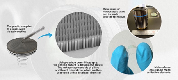
Previously, large-scale manufacturing of metasurfaces presented many obstacles. Advanced equipment is required for their manufacturing, and the process is quite time-consuming. However, using the method developed by the Chalmers researchers, the production rate can be increased several times compared to current state-of-the-art techniques.
The new technology uses harmless chemicals and machines common in nanomanufacturing laboratories today, meaning that more researchers could now begin to study metasurfaces.
“Our method could be a step toward large-scale production of metasurfaces,” said Ruggero Verre, a researcher at the Department of Physics at Chalmers and co-author of the paper. “That is the goal we are already working toward today. Metasurfaces can help us create different effects and offer various technological possibilities. The best is yet to come.”
The research was published in ACS Photonics (www.doi.org/10.1021/acsphotonics.9b01809).
