Jul 08, 2020
(Nanowerk News) Researchers at ARCNL have found a way to detect nanostructures buried under many layers of opaque material, using very high frequency sound waves induced by light. Their findings are promising in view of applications in the semiconductor manufacturing industry, such as wafer alignment. The researchers also revealed interesting new phenomena in photo-acoustics that have not been investigated before.
They published their results in Physical Review Applied ("Detection of hidden gratings through multilayer nanostructures using light and sound"). First author of the article, Stephen Edward successfully defended his PhD on this subject on 18 June at the University of Amsterdam.
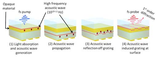 A femtosecond pump laser ‘knocks’ at the opaque material (1), causing a high frequency acoustic wave to travel through the layers (2) until it reaches the buried grating lines. The acoustic waves are reflected at the grating and travel back (3) as a grating shaped wave. When this wave hits the surface (4), the grating shaped deformation can be detected from the diffraction signal of a femtosecond probe laser. (Image: ARCNL) (click on image to enlarge)
In the production of state-of-the art computer chips and components, nanolithography machines print several layers of nano-size structures on a wafer. To make sure the layers are aligned accurately, wafers contain grating lines that act as markers that tell the machines where to print.
“While alignment markers are indispensable in nanolithography, they get buried under many layers of material. Because these layers are often opaque, it is difficult to use light to find the markers and align the machine”, says Stephen Edward, who carried out his PhD research in the Light-Matter Interaction group at ARCNL.
A femtosecond pump laser ‘knocks’ at the opaque material (1), causing a high frequency acoustic wave to travel through the layers (2) until it reaches the buried grating lines. The acoustic waves are reflected at the grating and travel back (3) as a grating shaped wave. When this wave hits the surface (4), the grating shaped deformation can be detected from the diffraction signal of a femtosecond probe laser. (Image: ARCNL) (click on image to enlarge)
In the production of state-of-the art computer chips and components, nanolithography machines print several layers of nano-size structures on a wafer. To make sure the layers are aligned accurately, wafers contain grating lines that act as markers that tell the machines where to print.
“While alignment markers are indispensable in nanolithography, they get buried under many layers of material. Because these layers are often opaque, it is difficult to use light to find the markers and align the machine”, says Stephen Edward, who carried out his PhD research in the Light-Matter Interaction group at ARCNL.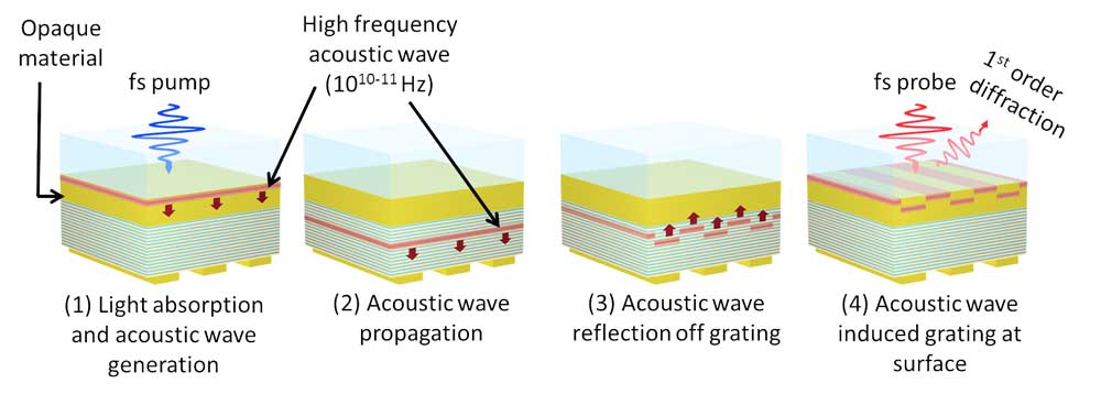
