| Date | 16th, Oct 2020 |
|---|
Home > Press > Bruker Launches Advanced In-Situ Nanomechanical Test Instrument for Analyzing Materials Deformation in Electron Microscopes: Hysitron PI 89 SEM PicoIndenter Offers Unprecedented Range and Flexibility
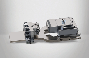
Abstract: The Bruker Nanomechanical Testing business today announced the release of the Hysitron PI 89 SEM PicoIndenter� to provide nanomechanical testing capabilities inside a scanning electron microscope (SEM) at higher loads and in more extreme environments than previously possible. This benefits researchers� understanding of the deformation mechanisms of high-strength materials. The new system combines Bruker�s high-performance controller with exclusive capacitive transducer and intrinsic displacement technologies to enable unmatched force and displacement ranges.
Minneapolis, MN | Posted on October 15th, 2020
The PI 89 SEM PicoIndenter is the first in-situ instrument with two rotation and tilt stage configurations. This enables flexible sample positioning toward the electron column for top-down imaging, tilting toward the FIB column for milling, spindle rotation for crystallographic alignment, and compatibility with a wide range of detectors to enable structure-property correlation of complex materials.
�The University of Alabama is excited to be the first recipient of Bruker�s Hysitron PI 89 SEM PicoIndenter in-situ nanomechanical testing unit,� said Dr. Gregory Thompson, Director of the Alabama Analytical Research Center. Professor of Mechanical Engineering Dr. Keivan Davami added, �The state-of-the-art capabilities of this platform to achieve extremes in temperature while simultaneously applying load will provide unprecedented structure characterization capture, including Transmission Kikuchi Diffraction and Electron Backscattered Diffraction, in support of multiple research programs.�
�The Hysitron PI 89 instrument is a compelling addition to our pioneering PicoIndenter Series for in-situ nanomechanical testing in electron microscopes,� stated Dr. Oden Warren, General Manager of Bruker�s Nanomechanical Testing business. �The new platform features superior versatility, ease of use, and stiffness to support higher loads, as well as several patented features to provide customers the widest range of testing flexibility and industry-leading performance in their SEMs. We are excited to see the new research this next-generation instrument makes possible.�
About the Hysitron PI 89 SEM PicoIndenter
The Hysitron PI 89 system is the latest generation of Bruker�s renowned family of Hysitron PicoIndenter test instruments for SEMs. Built upon Bruker's state-of-the-art capacitive transducer technology, PI 89 offers researchers an advanced instrument with powerful capabilities that delivers extraordinary performance and versatility. Its capabilities include automated nanoindentation, accelerated mechanical property mapping (XPM), fatigue testing, nanotribology, Push-to-Pull (PTP) tension for thin films and nanowires (patented), direct-pull tension, SPM imaging, an electrical characterization module, elevated temperature testing (patented), rotation and tilt stage (patented), and compatibility with analytical imaging using EBSD, EDS, CBD, TKD, and STEM detectors.
####
For more information, please click here
Contacts:Stephen Hopkins
Content Marketing Manager
Bruker Nano Surfaces and Metrology Division
T: +1 (520) 741-1044 x1022
E:
Copyright © Bruker Corporation
If you have a comment, please Contact us.
Issuers of news releases, not 7th Wave, Inc. or Nanotechnology Now, are solely responsible for the accuracy of the content.
Bookmark:


News and information
![]() New technology helps reveal inner workings of human genome June 24th, 2022
New technology helps reveal inner workings of human genome June 24th, 2022
![]() Boron nitride nanotube fibers get real: Rice lab creates first heat-tolerant, stable fibers from wet-spinning process June 24th, 2022
Boron nitride nanotube fibers get real: Rice lab creates first heat-tolerant, stable fibers from wet-spinning process June 24th, 2022
Imaging
![]() Snapshot measurement of single nanostructure�s circular dichroism March 25th, 2022
Snapshot measurement of single nanostructure�s circular dichroism March 25th, 2022
![]() Better understanding superconductors with Higgs spectroscopy Prof. Stefan Kaiser from TU Dresden awarded ERC Consolidator Grant March 18th, 2022
Better understanding superconductors with Higgs spectroscopy Prof. Stefan Kaiser from TU Dresden awarded ERC Consolidator Grant March 18th, 2022
![]() Visualizing the invisible: New fluorescent DNA label reveals nanoscopic cancer features March 4th, 2022
Visualizing the invisible: New fluorescent DNA label reveals nanoscopic cancer features March 4th, 2022
Announcements
![]() New technology helps reveal inner workings of human genome June 24th, 2022
New technology helps reveal inner workings of human genome June 24th, 2022
![]() Boron nitride nanotube fibers get real: Rice lab creates first heat-tolerant, stable fibers from wet-spinning process June 24th, 2022
Boron nitride nanotube fibers get real: Rice lab creates first heat-tolerant, stable fibers from wet-spinning process June 24th, 2022
Tools
![]() New technology helps reveal inner workings of human genome June 24th, 2022
New technology helps reveal inner workings of human genome June 24th, 2022
![]() Snapshot measurement of single nanostructure�s circular dichroism March 25th, 2022
Snapshot measurement of single nanostructure�s circular dichroism March 25th, 2022
![]() Eyebrow-raising: Researchers reveal why nanowires stick to each other February 11th, 2022
Eyebrow-raising: Researchers reveal why nanowires stick to each other February 11th, 2022
![]() JEOL Introduces New Scanning Electron Microscope with �Simple SEM� Automation and Live Elemental and 3D Analysis January 14th, 2022
JEOL Introduces New Scanning Electron Microscope with �Simple SEM� Automation and Live Elemental and 3D Analysis January 14th, 2022
New-Contracts/Sales/Customers
![]() Bruker Light-Sheet Microscopes at Major Comprehensive Cancer Center: New Advanced Imaging Center Powered by Two MuVi and LCS SPIM Microscopes March 25th, 2021
Bruker Light-Sheet Microscopes at Major Comprehensive Cancer Center: New Advanced Imaging Center Powered by Two MuVi and LCS SPIM Microscopes March 25th, 2021
![]() Arrowhead Pharmaceuticals Announces Closing of Agreement with Takeda November 27th, 2020
Arrowhead Pharmaceuticals Announces Closing of Agreement with Takeda November 27th, 2020
![]() Veeco Announces Aledia Order of 300mm MOCVD Equipment for microLED Displays: Propel� Platform First 300mm System with EFEM Designed for Advanced Display Applications October 20th, 2020
Veeco Announces Aledia Order of 300mm MOCVD Equipment for microLED Displays: Propel� Platform First 300mm System with EFEM Designed for Advanced Display Applications October 20th, 2020
![]() GREENWAVES TECHNOLOGIES Announces Next Generation GAP9 Hearables Platform Using GLOBALFOUNDRIES 22FDX Solution October 16th, 2020
GREENWAVES TECHNOLOGIES Announces Next Generation GAP9 Hearables Platform Using GLOBALFOUNDRIES 22FDX Solution October 16th, 2020
