| Date | 3rd, Dec 2020 |
|---|
Home > Press > New platform generates hybrid light-matter excitations in highly charged graphene
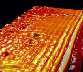 Massive work function-mediated charge transfer in graphene/?-RuCl3 heterostructures provides the necessary conditions for generating plasmon polaritons without electrostatic or chemical doping. The image depicts a characteristic infrared near-field image of such a heterostructure, revealing a host of plasmonic oscillations derived from substantial mutual doping of interfacial graphene/?-RuCl3 layers.
CREDIT
Daniel J. Rizzo/Columbia University
Massive work function-mediated charge transfer in graphene/?-RuCl3 heterostructures provides the necessary conditions for generating plasmon polaritons without electrostatic or chemical doping. The image depicts a characteristic infrared near-field image of such a heterostructure, revealing a host of plasmonic oscillations derived from substantial mutual doping of interfacial graphene/?-RuCl3 layers.
CREDIT
Daniel J. Rizzo/Columbia University
Abstract: Columbia researchers are the first to use static charge between 2D atomic layers to provide a new route for generating graphene plasmon polaritons without an external power source or chemical dopants; discovery has broad application in nanotechnology.
New York, NY | Posted on December 2nd, 2020
Graphene, an atomically thin carbon layer through which electrons can travel virtually unimpeded, has been extensively studied since its first successful isolation more than 15 years ago. Among its many unique properties is the ability to support highly confined electromagnetic waves coupled to oscillations of electronic charge--plasmon polaritons--that have potentially broad applications in nanotechnology, including biosensing, quantum information, and solar energy.
However, in order to support plasmon polaritons, graphene must be charged by applying a voltage to a nearby metal gate, which greatly increases the size and complexity of nanoscale devices. Columbia University researchers report that they have achieved plasmonically active graphene with record-high charge density without an external gate. They accomplished this by exploiting novel interlayer charge transfer with a two-dimensional electron-acceptor known as α-RuCl3. The study is available now online as an open access article and will appear in the December 9th issue of Nano Letters.
"This work allows us to use graphene as a plasmonic material without metal gates or voltage sources, making it possible to create stand-alone graphene plasmonic structures for the first time" said co-PI James Hone, Wang Fong-Jen Professor of Mechanical Engineering at Columbia Engineering.
All materials possess a property known as a work function, which quantifies how tightly they can hold on to electrons. When two different materials are brought into contact, electrons will move from the material with the smaller work function to the material with the larger work function, causing the former to become positively charged and the latter to become negatively charged. This is the same phenomenon that generates static charge when you rub a balloon against your hair.
α-RuCl3 is unique among nanomaterials because it has an exceptionally high work function even when it is exfoliated down to a one- or few-atom-thick 2D layers. Knowing this, the Columbia researchers created atomic-scale stacks consisting of graphene on top of α-RuCl3. As expected, electrons were removed from the graphene, making it highly conductive and able to host plasmon polaritons -- without the use on an external gate.
Using α-RuCl3 to charge graphene brings two main advantages over electrical gating. α-RuCl3 induces much greater charge than can be achieved with electrical gates, which are limited by breakdown of the insulating barrier with the graphene. In addition, the spacing between graphene and the underlying gate electrode blurs the boundary between charged and un-charged regions due to "electric field fringing." This prevents realization of sharp charge features within the graphene and along the graphene edge necessary to manifest novel plasmonic phenomena. In contrast, at the edge of the α-RuCl3, the charge in the graphene drops to zero on nearly the atomic scale.
"One of our major achievements in this work is attaining charge densities in graphene roughly 10 times larger than the limits imposed by dielectric breakdown in a standard gated device," said the study's lead PI Dmitri Basov, professor of physics. "Moreover, since the α-RuCl3--the source of electronic charge--is in direct contact with graphene, the boundaries between the charged and uncharged regions in the graphene are razor-sharp. This allows us to observe mirror-like plasmon reflection from these edges and to create historically elusive one-dimensional edge plasmons that propagate along the graphene edge." The team also observed sharp boundaries at "nano-bubbles," where contaminants trapped between the two layers disrupt charge transfer.
"We were very excited to see how abruptly the graphene charge density can change in these devices," said Daniel Rizzo, a postdoctoral research scientist with Basov and the lead author on the paper. "Our work is a proof-of-concept for nanometer charge control that was previously the realm of fantasy."
The work was carried out in the Energy and Frontier Research Center on Programmable Quantum Materials funded by the United States Department of Energy and led by Basov. The research project used shared facilities operated by the Columbia Nano Initiative.
The researchers are now pursuing routes to use etched α-RuCl3 as a platform for generating custom nanoscale charge patterns in graphene to precisely tune the plasmonic behavior according to various practical applications. They also hope to demonstrate that α-RuCl3 can be interfaced with a wide range of 2D materials to access novel material behaviors that require the exceptionally high charge density imparted by interlayer charge transfer demonstrated in their manuscript.
Hone noted, "When our interlayer charge transfer technique is combined with existing procedures for patterning 2D substrates, we can easily generate tailor-made nanoscale charge patterns in graphene. This opens up a wealth of new opportunities for new electronic and optical devices"
###
About the Study
The study is titled "Charge-Transfer Plasmon Polaritons at Graphene/α-RuCl3 Interfaces."
Authors are: Daniel J. Rizzo1, Bjarke S. Jessen1,2, Zhiyuan Sun1, Francesco L. Ruta1,3, Jin Zhang4, Jia-Qiang Yan5,6, Lede Xian4, Alexander S. McLeod1, Michael E. Berkowitz1, Kenji Watanabe7, Takashi Taniguchi8, Stephen E. Nagler9, David G. Mandrus5,6, Angel Rubio4,10,11, Michael M. Fogler12, Andrew J. Millis1,10, James C. Hone2, Cory R. Dean1, D.N. Basov1
1Department of Physics, Columbia University
2Department of Mechanical Engineering, Columbia Engineering
3Department of Applied Physics and Applied Mathematics, Columbia Engineering
4Theory Department, Max Planck Institute for Structure and Dynamics of Matter and Center for Free-Electron Laser Science, Hamburg, Germany
5Materials Science and Technology Division, Oak Ridge National Laboratory, Oak Ridge, Tennessee
6Department of Materials Science and Engineering, University of Tennessee, Knoxville,
7Research Center for Functional Materials, National Institute for Materials Science, Tsukuba, Japan
8International Center for Materials Nanoarchitectonics, National Institute for Materials Science, Tsukuba, Japan
9Neutron Scattering Division, Oak Ridge National Laboratory, Oak Ridge, Tennessee
10Center for Computational Quantum Physics, Flatiron Institute, New York
11Nano-Bio Spectroscopy Group, Universidad del Pa�s Vasco UPV/EHU, San Sebasti�n, Spain
12Department of Physics, University of California San Diego
This research at Columbia was supported as part of the Energy Frontier Research Center on Programmable Quantum Materials funded by the US Department of Energy (DOE), Office of Science, Basic Energy Sciences (BES), under award no. DE-SC0019443. The study was also funded by the European Research Council (ERC-2015-AdG694097), the Cluster of Excellence "Advanced Imaging of Matter" (AIM), Grupos Consolidados (IT1249-19) and SFB925 "Light induced dynamics and control of correlated quantum systems," the European Union Horizon 2020 research and innovation program under Marie Sklodowska-Curie Grant Agreement 886291 (PeSD-NeSL), the Max Planck Institute-New York City Center for Non-Equilibrium Quantum Phenomena, the Simons Foundation, the Gordon and Betty Moore Foundation's EPiQS Initiative, Grant GBMF9069, U.S. Department of Energy, Office of Science, Basic Energy Sciences, Materials Sciences and Engineering Division, the Elemental Strategy Initiative conducted by the MEXT, Japan, Grant Number JPMXP0112101001, JSPS KAKENHI Grant Number JP20H00354 and the CREST (JPMJCR15F3), the Division of Scientific User Facilities of the US DOE Basic Energy Sciences, and the Office of Naval Research grant N00014-18-1-2722. D.N.B. is the Vannevar Bush Faculty ONR-VB: N00014-19-1-2630 and Moore investigator in Quantum Materials EPIQS program #9455.
####
About Columbia EngineeringColumbia Engineering, based in New York City, is one of the top engineering schools in the U.S. and one of the oldest in the nation. Also known as The Fu Foundation School of Engineering and Applied Science, the School expands knowledge and advances technology through the pioneering research of its more than 220 faculty, while educating undergraduate and graduate students in a collaborative environment to become leaders informed by a firm foundation in engineering. The School's faculty are at the center of the University's cross-disciplinary research, contributing to the Data Science Institute, Earth Institute, Zuckerman Mind Brain Behavior Institute, Precision Medicine Initiative, and the Columbia Nano Initiative. Guided by its strategic vision, "Columbia Engineering for Humanity," the School aims to translate ideas into innovations that foster a sustainable, healthy, secure, connected, and creative humanity.
For more information, please click here
Contacts:Holly Evarts
347-453-7408
@CUSEAS
Copyright © Columbia Engineering
If you have a comment, please Contact us.
Issuers of news releases, not 7th Wave, Inc. or Nanotechnology Now, are solely responsible for the accuracy of the content.
Bookmark:


News and information
![]() New technology helps reveal inner workings of human genome June 24th, 2022
New technology helps reveal inner workings of human genome June 24th, 2022
![]() Boron nitride nanotube fibers get real: Rice lab creates first heat-tolerant, stable fibers from wet-spinning process June 24th, 2022
Boron nitride nanotube fibers get real: Rice lab creates first heat-tolerant, stable fibers from wet-spinning process June 24th, 2022
Graphene/ Graphite
![]() OCSiAl expands its graphene nanotube production capacities to Europe June 17th, 2022
OCSiAl expands its graphene nanotube production capacities to Europe June 17th, 2022
![]() Bumps could smooth quantum investigations: Rice University models show unique properties of 2D materials stressed by contoured substrates June 10th, 2022
Bumps could smooth quantum investigations: Rice University models show unique properties of 2D materials stressed by contoured substrates June 10th, 2022
![]() Nanotubes: a promising solution for advanced rubber cables with 60% less conductive filler June 1st, 2022
Nanotubes: a promising solution for advanced rubber cables with 60% less conductive filler June 1st, 2022
![]() Dynamic metasurfaces and metadevices empowered by graphene May 6th, 2022
Dynamic metasurfaces and metadevices empowered by graphene May 6th, 2022
Govt.-Legislation/Regulation/Funding/Policy
![]() Solving the solar energy storage problem with rechargeable batteries that can convert and store energy at once June 24th, 2022
Solving the solar energy storage problem with rechargeable batteries that can convert and store energy at once June 24th, 2022
![]() Boron nitride nanotube fibers get real: Rice lab creates first heat-tolerant, stable fibers from wet-spinning process June 24th, 2022
Boron nitride nanotube fibers get real: Rice lab creates first heat-tolerant, stable fibers from wet-spinning process June 24th, 2022
![]() UBCO researchers change the game when it comes to activity tracking: Flexible, highly sensitive motion device created by extrusion printing June 17th, 2022
UBCO researchers change the game when it comes to activity tracking: Flexible, highly sensitive motion device created by extrusion printing June 17th, 2022
![]() University of Illinois Chicago joins Brookhaven Lab's Quantum Center June 10th, 2022
University of Illinois Chicago joins Brookhaven Lab's Quantum Center June 10th, 2022
Possible Futures
![]() New technology helps reveal inner workings of human genome June 24th, 2022
New technology helps reveal inner workings of human genome June 24th, 2022
![]() Boron nitride nanotube fibers get real: Rice lab creates first heat-tolerant, stable fibers from wet-spinning process June 24th, 2022
Boron nitride nanotube fibers get real: Rice lab creates first heat-tolerant, stable fibers from wet-spinning process June 24th, 2022
Chip Technology
![]() Boron nitride nanotube fibers get real: Rice lab creates first heat-tolerant, stable fibers from wet-spinning process June 24th, 2022
Boron nitride nanotube fibers get real: Rice lab creates first heat-tolerant, stable fibers from wet-spinning process June 24th, 2022
![]() Controlled synthesis of crystal flakes paves path for advanced future electronics June 17th, 2022
Controlled synthesis of crystal flakes paves path for advanced future electronics June 17th, 2022
Optical computing/Photonic computing
![]() Photonic integrated erbium doped amplifiers reach commercial performance: Boosting light power revolutionizes communications and autopilots June 17th, 2022
Photonic integrated erbium doped amplifiers reach commercial performance: Boosting light power revolutionizes communications and autopilots June 17th, 2022
![]() Electron-phonon coupling assisted universal red luminescence of o-phenylenediamine-based CDs June 10th, 2022
Electron-phonon coupling assisted universal red luminescence of o-phenylenediamine-based CDs June 10th, 2022
Discoveries
![]() New technology helps reveal inner workings of human genome June 24th, 2022
New technology helps reveal inner workings of human genome June 24th, 2022
![]() Boron nitride nanotube fibers get real: Rice lab creates first heat-tolerant, stable fibers from wet-spinning process June 24th, 2022
Boron nitride nanotube fibers get real: Rice lab creates first heat-tolerant, stable fibers from wet-spinning process June 24th, 2022
Announcements
![]() New technology helps reveal inner workings of human genome June 24th, 2022
New technology helps reveal inner workings of human genome June 24th, 2022
![]() Boron nitride nanotube fibers get real: Rice lab creates first heat-tolerant, stable fibers from wet-spinning process June 24th, 2022
Boron nitride nanotube fibers get real: Rice lab creates first heat-tolerant, stable fibers from wet-spinning process June 24th, 2022
Interviews/Book Reviews/Essays/Reports/Podcasts/Journals/White papers/Posters
![]() Quantum network nodes with warm atoms June 24th, 2022
Quantum network nodes with warm atoms June 24th, 2022
![]() New technology helps reveal inner workings of human genome June 24th, 2022
New technology helps reveal inner workings of human genome June 24th, 2022
Grants/Sponsored Research/Awards/Scholarships/Gifts/Contests/Honors/Records
![]() Solving the solar energy storage problem with rechargeable batteries that can convert and store energy at once June 24th, 2022
Solving the solar energy storage problem with rechargeable batteries that can convert and store energy at once June 24th, 2022
![]() Boron nitride nanotube fibers get real: Rice lab creates first heat-tolerant, stable fibers from wet-spinning process June 24th, 2022
Boron nitride nanotube fibers get real: Rice lab creates first heat-tolerant, stable fibers from wet-spinning process June 24th, 2022
Photonics/Optics/Lasers
![]() Photonic integrated erbium doped amplifiers reach commercial performance: Boosting light power revolutionizes communications and autopilots June 17th, 2022
Photonic integrated erbium doped amplifiers reach commercial performance: Boosting light power revolutionizes communications and autopilots June 17th, 2022
![]() Marching to the Cadence of Electronics: Innovation A new paper in Nature validates technology developed by John Bowers and collaborators June 10th, 2022
Marching to the Cadence of Electronics: Innovation A new paper in Nature validates technology developed by John Bowers and collaborators June 10th, 2022
Research partnerships
![]() New technology helps reveal inner workings of human genome June 24th, 2022
New technology helps reveal inner workings of human genome June 24th, 2022
![]() Boron nitride nanotube fibers get real: Rice lab creates first heat-tolerant, stable fibers from wet-spinning process June 24th, 2022
Boron nitride nanotube fibers get real: Rice lab creates first heat-tolerant, stable fibers from wet-spinning process June 24th, 2022
