In application, the sensor embeds into living plant tissue, where it detects arsenic levels as low as 0.2 parts per billion (ppb). Readouts from the nanosensors are obtainable via portable (and often inexpensive electronics). The full system coverts a nongenetically modified plant to a fully functional environmental sensor.
The advance has applications in environmental monitoring and agriculture — arsenic is a common contaminant in crops such as rice and tea. Long-term exposure to the metal can cause cardiovascular disease and cancers, including those of the skin, bladder, and lung. Elevated arsenic levels in soil can result from mining and smelting and can harm plant life and inhibit growth.
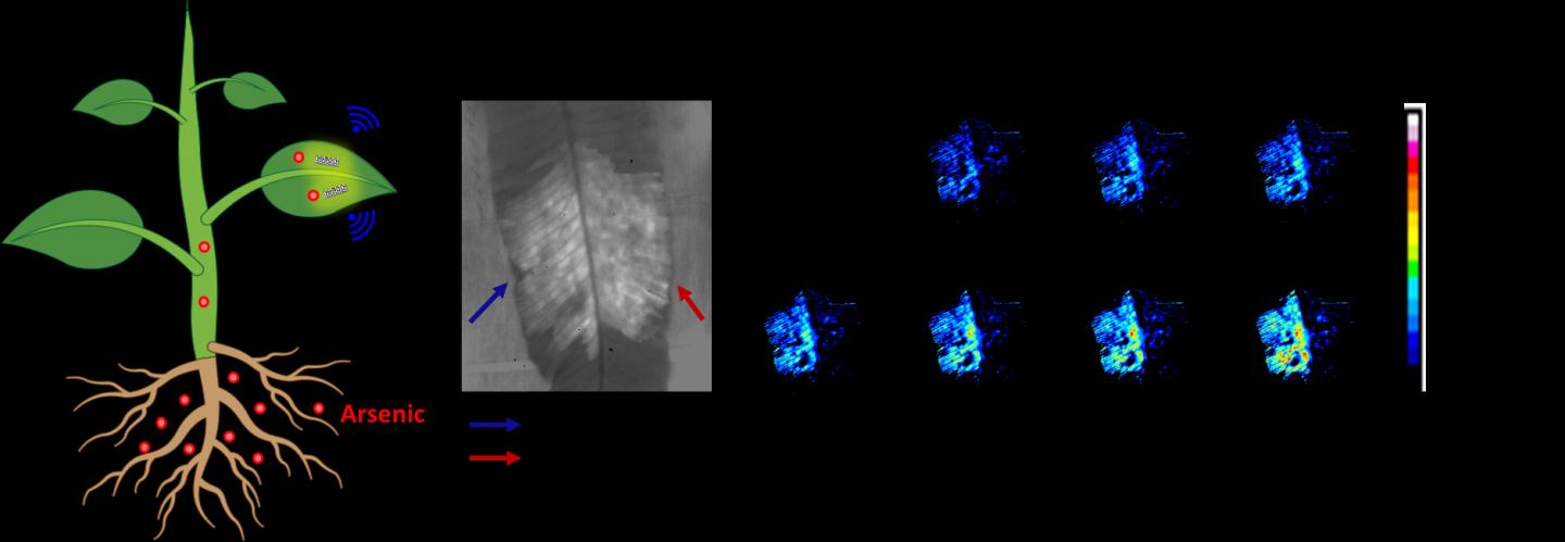
The researchers engineered single-walled carbon nanotubes and embedded the nanoparticles into living plant leaves. The single-walled nanotubes are fluorescent in the near-infrared range, located away from chlorophyll autofluorescence, Tedrick Thomas Salim Lew, lead author of the paper introducing the sensors, told Photonics Media. This ensured a high signal-to-noise ratio.
Lew said the surface of their distinct nanotubes can also be tuned to selectively detect arsenic-specific quantities, and that the nanotubes do not photobleach; their emission instead remains stable over time.
A charge-coupled camera, similar in performance to those found in a smartphone, paired with a portable Raspberry Pi platform, enabled real-time imaging and analysis using the nanotubes.
“Their fluorescence-change due to an interaction with arsenic was captured by both InGaAS detectors and a Raspberry Pi-coupled CCD camera in our study,” Lew said. “The latter demonstrated that our sensor can be monitored with portable, inexpensive electronics.”
The researchers tested on spinach and rice, as well as a species of fern that can hyperaccumulate arsenic. Because the fern species can absorb (and tolerate) high levels of arsenic without exhibiting detrimental effects, researchers were able to optimize their sensor devices to detect very low concentrations. The regulatory limit for existing arsenic detectors, the researchers said, is 10 ppb.
The researchers excited their sensors with a 785-nm laser and monitored the fluorescence intensity at a standoff distance of 1 m (away from the portable electronic devices). They positioned an emission filter in front of the CCD camera in the setup so that the camera only captured the fluorescence of the sensors, Lew said. The arrangement did not require components beyond the sensor, CCD camera, and filters.
With the sensors in place, scientists will additionally be able to develop and produce crops that are more resistant to toxic element uptakes, said MIT’s Michael Strano, co-author of the study describing the research and DiSTAP co-lead principal investigator. Work in that area is currently underway, he said, at Temasek Life Science Laboratory. Scientists at the research organization contributed to the current work.
“Any living plants can be converted into arsenic sensors,” Lew said. “An excitation source and camera without the infrared filter is needed to monitor the sensor fluorescence.”
Lew told Photonics Media that the researchers are now eyeing development of a miniaturized, portable, hand-held system capable of monitoring the fluorescence of the sensors within the plants. The new system would ensure that end users need not assemble any electronic of optical component.
“We are also evaluating the robustness and reliability of the sensors under field conditions outside of the laboratory,” said Lew. “Additionally, we are partnering with a research laboratory in Singapore to improve the utility of this platform in plant science research and agricultural applications.”
The National Research Foundation Singapore, under its Campus for Research Excellence And Technological Enterprise (CREATE) program, supported the research, which was published in Advanced Materials (www.doi.org/10.1002/adma.202005683).
