Light can only be focused down to a certain level, referred to as the Abbe limit. At this point, to a traditional optical microscope, objects that are closer than this limit would appear as one. Under certain conditions, however, these rules can be broken, using van der Waals crystals; these crystals are layered and possess semiconductor properties that allow for on-demand optical carrier injection.
In these specific instances, light can be confined without limit, enabling imaging of even the smallest of objects.
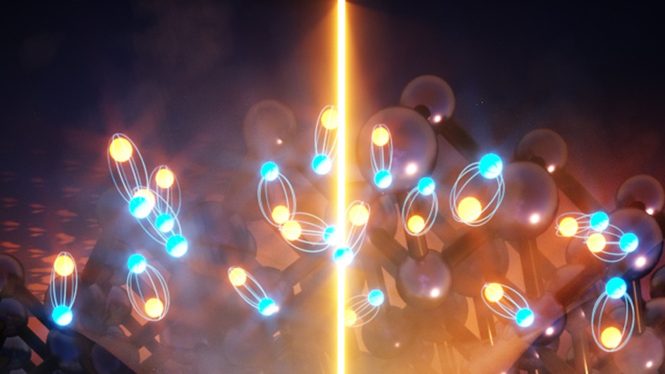
In terms of the crystal’s layered structure, the consequent strong anisotropy of the electronic structure is conducive for electronic hyperbolicity, or the ability to pass nanolight through its structure, said Aaron Sternbach, a graduate student in Columbia’s Department of Physics.
By illuminating the crystal with a pulse of light, the team changed the crystal’s electronic structure.
“The absorption process promotes electronic charge carriers, or electron-hole pairs, to an excited state. In the excited state, the charge carriers can reflect mid-infrared light, but since this is an anisotropic layered crystal, only light incident from the ‘top down’ is reflected while the crystal remains transmissive for light of the same frequency which is incident from the ‘side’ — which satisfies the precondition for hyperbolicity,” Sternbach told Photonics Media. “The best name I can think of for this process is ‘optical carrier injection.’”
The new structure arising from this reorganization enables superfine nanoscale details to be transported through the crystal where they could be imaged on the surface.
However, the technology isn’t without its drawbacks.
“A big challenge with hyperbolicity rooted in electronic processes is the relatively high loss within the crystals. Losses can be mitigated at low temperatures, or potentially in other crystals that are less sensitive to temperature-driven fluctuations,” Sternbach said. “Mitigating losses and thereby improving the photonic quality factors in hyperbolic crystals rooted in electronic processes are likely to be subjects of next-generation research.”
As far as next steps, because the discovery shows a method of accessing hyperbolic properties on demand and on ultrafast timescales, Sternbach believes that there will be more research efforts focusing on areas where light plays a dual role in programming quantum matter and in investigating emergent optically driven phases with nano-optics.
“We are also likely to see further reports where electronic forms of hyperbolicity are uncovered,” Sternbach said.
Dmitri Basov, the Higgins Professor of Physics at Columbia University and senior author on the research paper, expressed similar sentiment. “Laser pulses allowed us to create a new electronic state in this prototypical semiconductor, if only for a few picoseconds,” he said. “This discovery puts us on track toward optically programmable quantum phases in new materials.”
The research was published in Science (www.doi.org/10.1126/science.abe9163).
