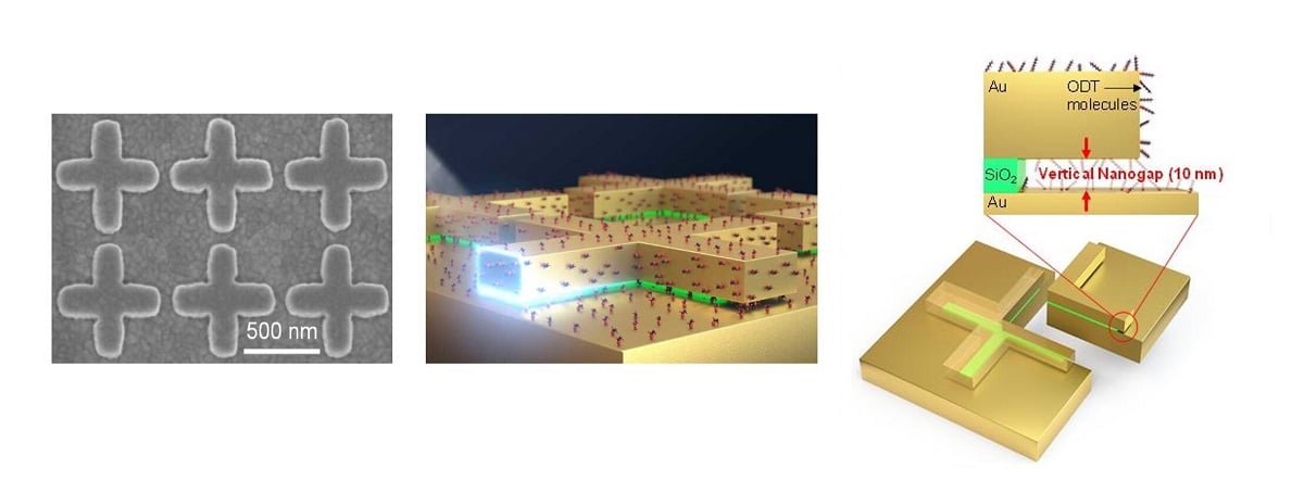
The material is able to enhance infrared absorption spectroscopy through hundredfold amplification of detection signals and features cross-shaped nano-antennas, formed in a metal-insulator-metal configuration. The middle insulating layer had a thickness of 10 nm, and the material’s designers employed vertical nanogaps — smaller than the wavelength of infrared light — to maximize light absorption by molecules.
Though high-resolution beam lithography was required to form the microstructure on metamaterial surfaces, the team’s surface enhanced infrared absorption (SEIRA) platform relies on more affordable nanoimprint lithography and dry-etching processes. The metamaterial may therefore be mass produced through affordable manufacturing processes.
“Using the nanoimprint process, we can obtain metamaterials in the metal-insulator-metal configuration and process them into desired patterns. On top of that, the dry-etching process allows mass production of microstructured metamaterials,” said Joo-Yun Jung, principal researcher at KIMM.
“Our study is the first to induce near-field enhancement and resolve near-field exposure using vertical gaps. The technique is expected to have vast applications, especially for infrared sensors used in the detection of biomolecules, harmful substances, and gases,” added UNIST professor Jongwon Lee.
The research was published in Small Methods (www.doi.org/10.1002/smtd.202100277).
