The technique is based on bound states of continuum. According to the researchers, it may pave the way to photonic integrated circuits (PICs).
“Silicon itself weakly interacts with light; it is a poor emitter and a poor absorber of photons. Therefore, taming silicon to interact with light effectively is an essential task,” Sergey Dyakov, senior researcher at Skoltech, said.
To increase PL in silicon, the researchers introduced bound states in the continuum into the emission process — a technique derived from quantum mechanics. They used a resonator based on bound states in the continuum that confined light effectively because the symmetry of the electromagnetic field inside the resonator did not correspond to the symmetry of the electromagnetic waves of the surrounding space.
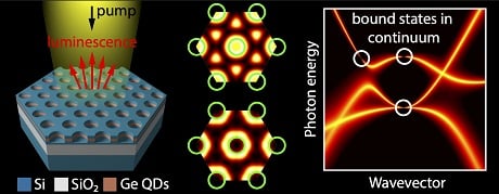
The researchers realized PL resonance peaks with a quality factor as high as 2200 and with a peak PL enhancement factor of more than two orders of magnitude. The corresponding integrated PL demonstrated PL enhancement of more than one order of magnitude.
“The use of bound states in the continuum increased luminescence intensity by more than a hundred times,” Dyakov said. The team did a theoretical study on the effect of bound states in the continuum using the Fourier modal method in the scattering matrix form.
Dakov believes that the work of the Russian team could open the way for CMOS-compatible photonic integrated circuits, improving CMOS performance by lessening the heat release caused by the density of elements in CMOS circuits. The ability to switch from metallic to optical connections between the elements could reduce heat generation because unlike electrons, photons can travel for huge distances with minimal heat losses.
Silicon today remains the leading material for the development and manufacture of chips, and most digital microcircuits are created using CMOS technology. Heat release due to high density of elements in CMOS circuits has contributed directly to the inability to further increase device performance.
One potential workaround is reducing heat generation by switching from metallic connections between elements in microcircuits to optical ones. Unlike electrons in conductors, photons can travel great distances in waveguides with minimal heat losses.
“The results open up new possibilities for creating efficient radiation sources based on silicon, built into the circuits of modern microelectronics with optical signal processing,” said professor Nikolay Gippius, head of the nanophotonics theory group at the Center of Photonics and Quantum Materials at Skoltech. “There are currently lots of groups working on creating light-emitting diodes based on such structures and the principles of their coupling with other elements on an optoelectronic chip.”
The research was published in Laser & Photonics Reviews (www.doi.org/10.1002/lpor.202000242).
