| Date | 14th, Aug 2021 |
|---|
Home > Press > Patterning silicon at the one nanometer scale: Scientists engineer materials� electrical and optical properties with plasmon engineering
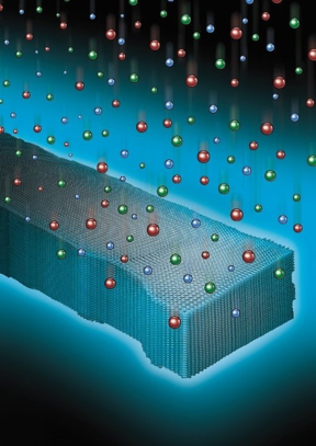 Ions from a reactive plasma shape a silicon nanowire approximately 40 atoms wide. The periodic atomic arrangement is preserved up to the edge of the nanowire.
CREDIT
Image courtesy of V.R. Manfrinato et al., Patterning Si at the 1 nm Length Scale with Aberration-Corrected Electron-Beam Lithography: Tuning of Plasmonic Properties by Design, Adv. Funct. Mater. 2019 1903429. Wiley-VCH GmbH. Reproduced with permission.
Ions from a reactive plasma shape a silicon nanowire approximately 40 atoms wide. The periodic atomic arrangement is preserved up to the edge of the nanowire.
CREDIT
Image courtesy of V.R. Manfrinato et al., Patterning Si at the 1 nm Length Scale with Aberration-Corrected Electron-Beam Lithography: Tuning of Plasmonic Properties by Design, Adv. Funct. Mater. 2019 1903429. Wiley-VCH GmbH. Reproduced with permission.
Abstract: The ScienceResearchers have developed an innovative technique for creating nanomaterials. These are materials only atoms wide. They draw on nanoscience to allow scientists to control their construction and behavior. The new electron beam nanofabrication technique is called plasmon engineering. It achieves unprecedented near-atomic scale control of patterning in silicon. Structures built using this approach produce record-high tuning of electro-optical properties.
Washington, DC | Posted on August 13th, 2021
The ImpactIn this research, scientists used plasmon engineering to control the optical and electronic properties of silicon. The technique uses aberration-corrected electron beam lithography. This process involves using a beam of electrons to modify the surface of a material. Plasmon engineering allowed researchers to modify material at the near atomic scale. The use of �conventional� lithography means this approach could one day be applied to industrial applications. This approach will benefit researchers working on optical communications, sensing, and quantum computing.
SummaryPatterning materials at single nanometer resolution allows scientists to precisely engineer quantum confinement effects. Quantum effects are significant at these length scales and controlling the nanostructure dimensions provides direct control over electrical and optical properties. Silicon is by far the most widely-used semiconductor material in electronics, and the ability to fabricate silicone‐based devices of the smallest dimensions for novel device engineering is highly desirable. Researchers at Brookhaven�s Center for Functional Nanomaterials, a Department of Energy user facility, used aberration‐corrected electron‐beam lithography combined with dry reactive ion etching to achieve patterning of 1 nanometer features as well as surface and volume plasmon engineering in silicon. The nanofabrication technique employed here produces nanowires with a line edge roughness of 1 nanometer. In addition, this work demonstrates tuning of the silicon volume plasmon energy by 1.2 electron volt from the bulk value, which is ten times higher than previous attempts of volume plasmon engineering using lithographic methods.
FundingThis research was supported by the DOE Office of Science and used resources at the Center for Functional Nanomaterials, an Office of Science user facility at Brookhaven National Laboratory.
####
For more information, please click here
Contacts:Michael Church
Office: 505-358-1481
Copyright © U.S. Department of Energy
If you have a comment, please Contact us.
Issuers of news releases, not 7th Wave, Inc. or Nanotechnology Now, are solely responsible for the accuracy of the content.
Bookmark:


News and information
![]() University of Illinois Chicago joins Brookhaven Lab's Quantum Center June 10th, 2022
University of Illinois Chicago joins Brookhaven Lab's Quantum Center June 10th, 2022
![]() Organic water splitters get a boost June 10th, 2022
Organic water splitters get a boost June 10th, 2022
Laboratories
![]() University of Illinois Chicago joins Brookhaven Lab's Quantum Center June 10th, 2022
University of Illinois Chicago joins Brookhaven Lab's Quantum Center June 10th, 2022
Nanofabrication
![]() First integrated laser on lithium niobate chip: Research paves the way for high-powered telecommunication systems April 8th, 2022
First integrated laser on lithium niobate chip: Research paves the way for high-powered telecommunication systems April 8th, 2022
![]() Atom by atom: building precise smaller nanoparticles with templates March 4th, 2022
Atom by atom: building precise smaller nanoparticles with templates March 4th, 2022
![]() Review on the femtosecond laser precision micro/nano-engineering December 3rd, 2021
Review on the femtosecond laser precision micro/nano-engineering December 3rd, 2021
![]() New tech builds ultralow-loss integrated photonic circuits April 16th, 2021
New tech builds ultralow-loss integrated photonic circuits April 16th, 2021
Plasmonics
![]() A new dimension in magnetism and superconductivity launched November 5th, 2021
A new dimension in magnetism and superconductivity launched November 5th, 2021
Govt.-Legislation/Regulation/Funding/Policy
![]() University of Illinois Chicago joins Brookhaven Lab's Quantum Center June 10th, 2022
University of Illinois Chicago joins Brookhaven Lab's Quantum Center June 10th, 2022
![]() Bumps could smooth quantum investigations: Rice University models show unique properties of 2D materials stressed by contoured substrates June 10th, 2022
Bumps could smooth quantum investigations: Rice University models show unique properties of 2D materials stressed by contoured substrates June 10th, 2022
![]() Nanostructured fibers can impersonate human muscles June 3rd, 2022
Nanostructured fibers can impersonate human muscles June 3rd, 2022
Possible Futures
![]() Electron-phonon coupling assisted universal red luminescence of o-phenylenediamine-based CDs June 10th, 2022
Electron-phonon coupling assisted universal red luminescence of o-phenylenediamine-based CDs June 10th, 2022
![]() Marching to the Cadence of Electronics: Innovation A new paper in Nature validates technology developed by John Bowers and collaborators June 10th, 2022
Marching to the Cadence of Electronics: Innovation A new paper in Nature validates technology developed by John Bowers and collaborators June 10th, 2022
![]() Small materials may be key to reducing cardiovascular disease deaths, researchers say June 10th, 2022
Small materials may be key to reducing cardiovascular disease deaths, researchers say June 10th, 2022
![]() Decoding a key part of the cell, atom by atom June 10th, 2022
Decoding a key part of the cell, atom by atom June 10th, 2022
Optical computing/Photonic computing
![]() Electron-phonon coupling assisted universal red luminescence of o-phenylenediamine-based CDs June 10th, 2022
Electron-phonon coupling assisted universal red luminescence of o-phenylenediamine-based CDs June 10th, 2022
![]() Marching to the Cadence of Electronics: Innovation A new paper in Nature validates technology developed by John Bowers and collaborators June 10th, 2022
Marching to the Cadence of Electronics: Innovation A new paper in Nature validates technology developed by John Bowers and collaborators June 10th, 2022
![]() Lightening up the nanoscale long-wavelength optoelectronics May 13th, 2022
Lightening up the nanoscale long-wavelength optoelectronics May 13th, 2022
![]() On-Chip Photodetection: Two-dimensional material heterojunctions hetero-integration May 13th, 2022
On-Chip Photodetection: Two-dimensional material heterojunctions hetero-integration May 13th, 2022
Discoveries
![]() Electron-phonon coupling assisted universal red luminescence of o-phenylenediamine-based CDs June 10th, 2022
Electron-phonon coupling assisted universal red luminescence of o-phenylenediamine-based CDs June 10th, 2022
![]() Marching to the Cadence of Electronics: Innovation A new paper in Nature validates technology developed by John Bowers and collaborators June 10th, 2022
Marching to the Cadence of Electronics: Innovation A new paper in Nature validates technology developed by John Bowers and collaborators June 10th, 2022
![]() Small materials may be key to reducing cardiovascular disease deaths, researchers say June 10th, 2022
Small materials may be key to reducing cardiovascular disease deaths, researchers say June 10th, 2022
![]() Decoding a key part of the cell, atom by atom June 10th, 2022
Decoding a key part of the cell, atom by atom June 10th, 2022
Materials/Metamaterials
![]() Nanotubes: a promising solution for advanced rubber cables with 60% less conductive filler June 1st, 2022
Nanotubes: a promising solution for advanced rubber cables with 60% less conductive filler June 1st, 2022
![]() New route to build materials out of tiny particles May 27th, 2022
New route to build materials out of tiny particles May 27th, 2022
![]() A one-stop shop for quantum sensing materials May 27th, 2022
A one-stop shop for quantum sensing materials May 27th, 2022
Announcements
![]() Organic water splitters get a boost June 10th, 2022
Organic water splitters get a boost June 10th, 2022
Interviews/Book Reviews/Essays/Reports/Podcasts/Journals/White papers/Posters
![]() Decoding a key part of the cell, atom by atom June 10th, 2022
Decoding a key part of the cell, atom by atom June 10th, 2022
![]() Organic water splitters get a boost June 10th, 2022
Organic water splitters get a boost June 10th, 2022
Photonics/Optics/Lasers
![]() Marching to the Cadence of Electronics: Innovation A new paper in Nature validates technology developed by John Bowers and collaborators June 10th, 2022
Marching to the Cadence of Electronics: Innovation A new paper in Nature validates technology developed by John Bowers and collaborators June 10th, 2022
![]() Lightening up the nanoscale long-wavelength optoelectronics May 13th, 2022
Lightening up the nanoscale long-wavelength optoelectronics May 13th, 2022
![]() On-Chip Photodetection: Two-dimensional material heterojunctions hetero-integration May 13th, 2022
On-Chip Photodetection: Two-dimensional material heterojunctions hetero-integration May 13th, 2022
![]() Small microring array enables large complex-valued matrix multiplication May 13th, 2022
Small microring array enables large complex-valued matrix multiplication May 13th, 2022
