| Date | 4th, Dec 2021 |
|---|
Home > Press > Review on the femtosecond laser precision micro/nano-engineering
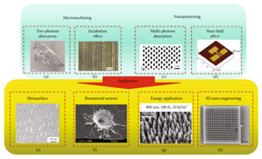 Femtosecond laser precision engineering strategies and the related applications: (a) bull sculpture produced by TPA, the scale bar is 2 μm, (b) microhole array fabricated on 150 μm Al film by femtosecond laser direct scanning, (c) wet etching of nanopores fabricated by 3D femtosecond laser writing in YAG crystal, (d) negative metal oxide semiconductor patterns fabricated by femtosecond laser assisting NSOM, (e) functional microstructures made by parallel femtosecond laser processing, (f) surface morphology of HP-PCL achieved by femtosecond laser microperforation, (g) SEM image of laser microstructured Si surface formed in SF6 with femtosecond laser pulses, and (h) 3D functional photonic crystal fabricated using 1030 nm femtosecond laser in a SZ2080 photoresist without using of photo initiator.
CREDIT
Ultrafast Science
Femtosecond laser precision engineering strategies and the related applications: (a) bull sculpture produced by TPA, the scale bar is 2 μm, (b) microhole array fabricated on 150 μm Al film by femtosecond laser direct scanning, (c) wet etching of nanopores fabricated by 3D femtosecond laser writing in YAG crystal, (d) negative metal oxide semiconductor patterns fabricated by femtosecond laser assisting NSOM, (e) functional microstructures made by parallel femtosecond laser processing, (f) surface morphology of HP-PCL achieved by femtosecond laser microperforation, (g) SEM image of laser microstructured Si surface formed in SF6 with femtosecond laser pulses, and (h) 3D functional photonic crystal fabricated using 1030 nm femtosecond laser in a SZ2080 photoresist without using of photo initiator.
CREDIT
Ultrafast Science
Abstract: Femtosecond laser precision engineering has been applied in industries for device micro/nano-fabrication due to its unique advantages of being a dry and noncontact process, coupled with the availability of reliable light sources and affordable system cost. It is an important advanced manufacturing means for high quality micro/nano-structures creation and related surface processing, especially to create new functional MEM/NEM devices and structures.
Shaanxi, P.R.China | Posted on December 3rd, 2021
Prof. Hong Minghui's research group at the National University of Singapore summarizes the development and latest progress of laser precision engineering from micron, sub-micron, to nanoscale. Combined with other advanced processing tools, femtosecond laser precision engineering�s resolution has been much smaller than the optical diffraction limit, which will play an important role in next-generation nano-manufacturing. For the micron-scale creation, the widely employed femtosecond laser fabrication strategies, including two/multi-photons absorption, laser-induced plasma-assisted ablation, and incubation effect are highlighted.
Furthermore, the recent progress about micro-lens arrays and interference lithography techniques for the sub-micron feature creation, especially large area periodic surface structuring, are also discussed. For the femtosecond laser nano-fabrication, both the processing strategies working in near field and far field are summarized.
The outlook of femtosecond laser precision engineering is also evaluated. How to achieve small heat affected zone is the first key issue in high quality laser precision engineering to push its resolution from micro-scale to nano-scale. Secondly, ensuring a high enough processing speed to meet various industrial needs is also a key challenge since one beam laser processing at high resolution could not meet this requirement. The third challenge is how to carry out the laser nano-structuring in the far field as the near field effect requires tiny optics working very close to sample surfaces, which confines the near field laser nano-fabrication to be only suitable for a few super-smooth surface samples.
####
For more information, please click here
Contacts:Jiangbo SheUltrafast Science
Copyright © Ultrafast Science
If you have a comment, please Contact us.
Issuers of news releases, not 7th Wave, Inc. or Nanotechnology Now, are solely responsible for the accuracy of the content.
Bookmark:


News and information
![]() �Fruitcake� structure observed in organic polymers June 3rd, 2022
�Fruitcake� structure observed in organic polymers June 3rd, 2022
![]() Progressive Medicinal and Herbal Nanoscience for Targeted Drug Delivery Systems June 3rd, 2022
Progressive Medicinal and Herbal Nanoscience for Targeted Drug Delivery Systems June 3rd, 2022
![]() Artificial Intelligence Centered Cancer Nanomedicine: Diagnostics, Therapeutics and Bioethics June 3rd, 2022
Artificial Intelligence Centered Cancer Nanomedicine: Diagnostics, Therapeutics and Bioethics June 3rd, 2022
Nanofabrication
![]() First integrated laser on lithium niobate chip: Research paves the way for high-powered telecommunication systems April 8th, 2022
First integrated laser on lithium niobate chip: Research paves the way for high-powered telecommunication systems April 8th, 2022
![]() Atom by atom: building precise smaller nanoparticles with templates March 4th, 2022
Atom by atom: building precise smaller nanoparticles with templates March 4th, 2022
![]() Patterning silicon at the one nanometer scale: Scientists engineer materials� electrical and optical properties with plasmon engineering August 13th, 2021
Patterning silicon at the one nanometer scale: Scientists engineer materials� electrical and optical properties with plasmon engineering August 13th, 2021
![]() New tech builds ultralow-loss integrated photonic circuits April 16th, 2021
New tech builds ultralow-loss integrated photonic circuits April 16th, 2021
Possible Futures
![]() Nanoscale bowtie antenna under optical and electrical excitations June 3rd, 2022
Nanoscale bowtie antenna under optical and electrical excitations June 3rd, 2022
![]() Emerging vaccine nanotechnology June 3rd, 2022
Emerging vaccine nanotechnology June 3rd, 2022
![]() �Fruitcake� structure observed in organic polymers June 3rd, 2022
�Fruitcake� structure observed in organic polymers June 3rd, 2022
![]() Progressive Medicinal and Herbal Nanoscience for Targeted Drug Delivery Systems June 3rd, 2022
Progressive Medicinal and Herbal Nanoscience for Targeted Drug Delivery Systems June 3rd, 2022
Discoveries
![]() Nanoscale bowtie antenna under optical and electrical excitations June 3rd, 2022
Nanoscale bowtie antenna under optical and electrical excitations June 3rd, 2022
![]() Emerging vaccine nanotechnology June 3rd, 2022
Emerging vaccine nanotechnology June 3rd, 2022
![]() �Fruitcake� structure observed in organic polymers June 3rd, 2022
�Fruitcake� structure observed in organic polymers June 3rd, 2022
Announcements
![]() �Fruitcake� structure observed in organic polymers June 3rd, 2022
�Fruitcake� structure observed in organic polymers June 3rd, 2022
![]() Progressive Medicinal and Herbal Nanoscience for Targeted Drug Delivery Systems June 3rd, 2022
Progressive Medicinal and Herbal Nanoscience for Targeted Drug Delivery Systems June 3rd, 2022
![]() Artificial Intelligence Centered Cancer Nanomedicine: Diagnostics, Therapeutics and Bioethics June 3rd, 2022
Artificial Intelligence Centered Cancer Nanomedicine: Diagnostics, Therapeutics and Bioethics June 3rd, 2022
Interviews/Book Reviews/Essays/Reports/Podcasts/Journals/White papers/Posters
![]() �Fruitcake� structure observed in organic polymers June 3rd, 2022
�Fruitcake� structure observed in organic polymers June 3rd, 2022
![]() Progressive Medicinal and Herbal Nanoscience for Targeted Drug Delivery Systems June 3rd, 2022
Progressive Medicinal and Herbal Nanoscience for Targeted Drug Delivery Systems June 3rd, 2022
![]() Artificial Intelligence Centered Cancer Nanomedicine: Diagnostics, Therapeutics and Bioethics June 3rd, 2022
Artificial Intelligence Centered Cancer Nanomedicine: Diagnostics, Therapeutics and Bioethics June 3rd, 2022
Photonics/Optics/Lasers
![]() Lightening up the nanoscale long-wavelength optoelectronics May 13th, 2022
Lightening up the nanoscale long-wavelength optoelectronics May 13th, 2022
![]() On-Chip Photodetection: Two-dimensional material heterojunctions hetero-integration May 13th, 2022
On-Chip Photodetection: Two-dimensional material heterojunctions hetero-integration May 13th, 2022
![]() Small microring array enables large complex-valued matrix multiplication May 13th, 2022
Small microring array enables large complex-valued matrix multiplication May 13th, 2022
