Pulsed laser systems have been used for 3D printing because they support two-photon absorption — that is, the simultaneous absorption of two photons to excite a molecule from one state to a state of higher energy. Two-photon absorption triggers a chemical reaction that hardens material into a 3D-printed structure. Complex laser systems are used to induce simultaneous excitation of molecules through two-photon absorption. Although femtosecond lasers enable efficient two-photon absorption, they come with drawbacks, including higher-order processes, cost, reliability issues, and size.
In the two-step absorption process developed by the KIT-Heidelberg team, one photon transfers the molecule to an intermediate state. Then, a second photon transfers the molecule from the intermediate state to the excited state. The molecule in its excited state prompts the chemical reaction needed to print the 3D structure. Unlike two-photon absorption, the photons in the two-step process do not need to be absorbed simultaneously.
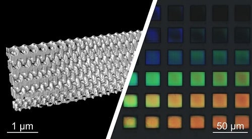
The researchers said that under suitable conditions, two-step absorption shows the same quadratic optical nonlinearity as two-photon absorption. The printing process requires specific photoresists. The researchers, in collaboration with chemists, developed a photoresist system. The system is based on a photo-initiator that supports two-step absorption.
“For the process, compact and low-power continuous-wave laser diodes can be used,” researcher Vincent Hahn said.
Demonstrations showed that the two-step absorption system can be used for printing state-of-the-art 3D nanostructures. In experiments, the team used about 100 μW of optical power from an inexpensive, compact, continuous-wave semiconductor laser diode emitting at 405 nm. Hahn believes that the two-step process works even better than traditional two-photon absorption.
“It is a big difference between using a femtosecond laser as large as a big suitcase for several €10,000 or a semiconductor laser that is as large as a pinhead and costs less than €10,” said Martin Wegener, a professor at KIT and an author of the research paper.
The researchers plan to miniaturize the other components of the 3D laser nanoprinter. “To me, a device that will be as large as a shoebox appears realistic in the next years,” Wegener said. “That would be even smaller than the laser printer on my desktop at KIT.”
The two-step absorption process could spur radical miniaturization — accompanied by a radical cost reduction — of 3D laser nanoprinters, making them affordable to a greater population.
The research was published in Nature Photonics (www.doi.org/10.1038/s41566-021-00906-8).
