In nanodevice fabrication, some applications require nanostructures with uniform feature sizes, while others require structures with spatially varying morphologies. In applications in optoelectronics, plasmonics, meta-optics, biosensing, and other technologies, precise control of feature size is essential.
In its approach, the team used high-throughput interference lithography (IL) to efficiently fabricate large-area periodic nanostructures. IL exposes a large-area periodic nanoscale pattern on the photoresist substrate. The researchers then applied a secondary exposure (SE) of UV light, which carries a designed intensity distribution of a grayscale pattern, to the IL-exposed photoresist. This step allows the researchers to spatially modulate the feature sizes of individual nanostructures.
To support wafer-scale nanostructure patterning with improved uniformity, IL-GPSE compensates for the linewidth variation caused by the nonuniform IL exposure field by using a specially designed SE intensity distribution.
The researchers tested the reliability of their technique through experiments and numerical simulation. Using UV contact photolithography, maskless projection photolithography, and direct laser writing for SE, they demonstrated feature size modulation with submicron resolution and for a wafer-scale area.
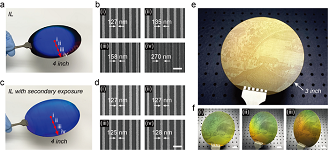
Additionally, the researchers demonstrated a 3-in. wafer-scale structural color painting by spatially modulating the filling ratio of the nanostructures to achieve gradient grayscale color using SE. IL-GPSE enabled precise grayscale control, demonstrating that it could be used for potential applications in flat optical devices and structural color encryption.
The researchers said that traditional methods for controlling feature size in nanostructures are unable to simultaneously provide high throughput, control over a large area, and precise feature size control in nanopatterning.
The IL-GPSE process portfolio could significantly improve the process of fabricating nanostructures that require spatially varying dimensions.
“Wafer-scale nanodevices fabricated by the presented technique can benefit a wide variety of applications,” the researchers said. “For example, large-area uniform nanogratings can be used in spectroscopy, astronomy, lasers, etc. Large-area structural color attracts broader applications in high-definition displays, anti-counterfeiting, sensing, etc.”
The IL-GPSE lithographic portfolio could also be applied to the fabrication of metasurfaces and metalenses that employ nanostructures with spatially modulated filling ratios. By separating the high-resolution patterning of metasurface building blocks and the size modulation, IL-GPSE has the potential to improve the patterning efficiency for these devices by orders of magnitude, compared to electron beam lithography.
The research was led by HKU professor Wen-Di Li. The research was published in Light: Science & Applications (www./doi.org/10.1038/s41377-022-00774-z).
