

| Date | 23rd, May 2022 |
|---|
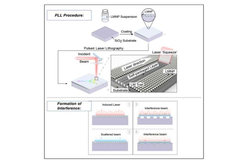 Laser interference lithography is invented for nano-patterning liquid metal (LM). The resolution in LM patterns breaks the optical limit of laser beams. Pulsed-laser-induced compression enables uniform 500-nm LM nanolayers. The robust oxide shell on LM boosts the mechanical properties and reliability. Credit: Matter (2022). DOI: 10.1016/j.matt.2022.01.004
In a new report now published in Matter, Licong An, and a team of scientists in materials engineering, industrial engineering, and the nanotechnology center at Purdue University, U.S., and Wuhan University, China, described an advanced laser lithography method. The technique facilitated the formation of electronically self-protective liquid metal patterns with feature sizes in the sub-microscale, to form one of the highest resolution metal surface patterns to date. The unique structure and robust patterns offered electrical functionality in spite of external damage. Such high-resolution, electrical, self-protective materials are suited for next-generation nano applications.
Introducing a new method: Pulsed laser lithography (PLL)
The field of high-density electronics is of great significance in materials engineering, and is suited to form high-density patterns for integrated electronics in harsh environments. Materials and industrial scientists have used room-temperature gallium indium (EGaIn) to develop high-density patterns due to their distinct properties including high fluidity, high electrical conductivity and high deformability. Research efforts to develop high-resolution liquid metal patterns are based on lithography patterning, among a diverse range of methods, with broad appeal in electronic applications across liquid metal batteries, microfluidics and energy harvesting devices.
In this work, primary author and research associate Licong An, who is presently at the materials engineering department at Purdue University, described the method as a "practical and scalable technique to fabricate self-packaged, high-resolution liquid metal patterns." The team intend to "practically integrate electric chips for use in harsh environments." The scientists primarily introduced the pulsed laser lithography method in this work to develop 3D liquid metal patterns with sub-micron level resolution, protected via a mechanically stable oxide package shell. Licong An highlighted the significance of this approach: "For the first time, the one-step lithography method can be directly used to pattern liquid metal," he said.
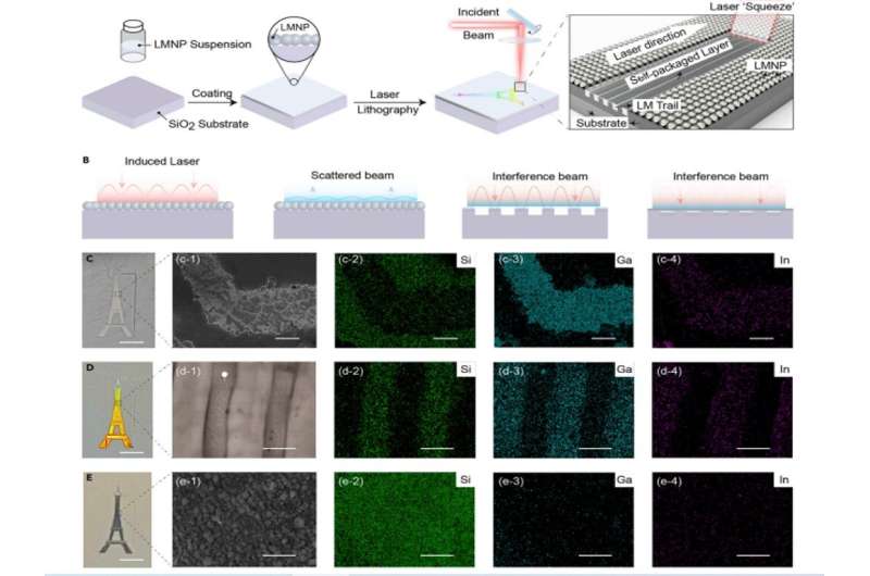 Schematic of the formation of liquid metal nano-patterns and surface morphologies of laser-treated samples. (A) Schematic of high-resolution liquid metal nano-pattern formation. (B) Schematic of the formation of interference beam and laser lithography-induced liquid metal nano-patterns. (C) Surface morphology and EDX mapping of the sample after laser sintering. Scale bar, 0.5 cm in (C) and 10 mm in (c-1, c-2, c-3, c-4). (D) Surface morphology and EDX mapping of the sample after laser lithography. The white dots in (d-1) indicate the ablation-induced oxide nanoparticle assemblies. Scale bar, 0.5 cm in (D) and 500 nm in (d-1, d-2, d-3, d-4). (E) Surface morphology and EDX mapping of the sample after laser ablation. Scale bar, 0.5 cm in (E) and 500 nm in (e-1, e-2, e-3, e-4). Credit: Matter (2022). DOI: 10.1016/j.matt.2022.01.004
He further defined the practical implications of the method "due to the high surface tension and flowing patterns, when compared to traditional lithography patterning. This is the first time that a lithography method is used to directly pattern liquid metals." The work described here is therefore "a first effort to introduce advanced laser lithography as a one-step process to directly generate highly efficient liquid metal patterns," he said.
The experiments: Liquid metal nanoparticle (LMNP) development
The research team summarized the method of developing high-resolution liquid metal patterns in four steps. At first, they sprayed a liquid metal nanoparticle (LMNP) onto a substrate to form an LMNP thin film. Then focused the pulsed laser beam on the thin film surface, where the incidence beam scattered due to its surface nanostructure, followed by ablation of the LMNPs and substrate where the peak energy intensity reached an ablation threshold. The laser-induced shock acted as a squeeze to generate pressure on the liquid metal particles and the team used laser energy as the main parameter to control the formation of high-resolution patterns. The team regulated the ultrafast heating and cooling rate by laser, to generate a 3D uniform oxide layer on the top surface of the 3D architecture, with boosted mechanical stability, for high stability in the face of exterior damage.
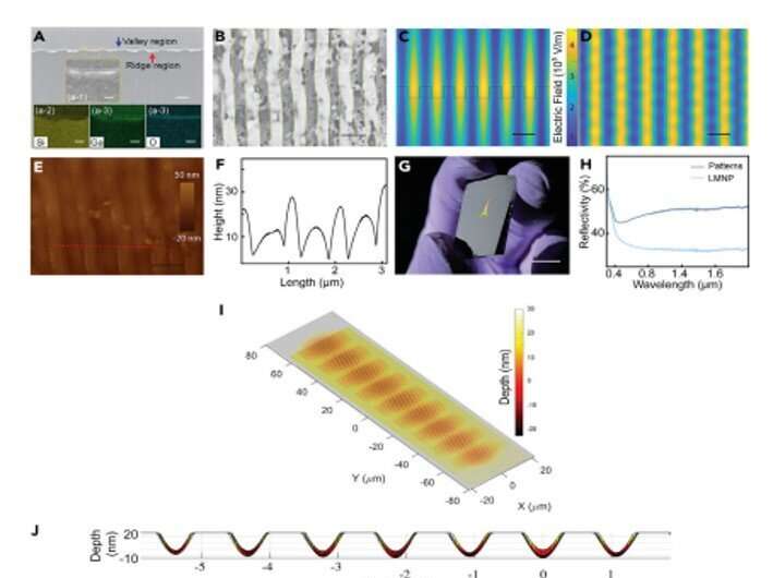 Characterization of the liquid metal nano-patterns. (A) Cross-section view and EDX mapping of liquid metal nano-patterns. Scale bar, 500 nm. (a-1) is one zoomed-in pattern, (a-2) (a-4) are the EDX mappings of the single pattern. Scale bar from (a-1) to (a-4), 100 nm. (B) Surface morphology of liquid metal nano-patterns. Scale bar, 1 mm. (C and D) Interference electric field from the incident beam and the liquid metal scattered fields in the vertical cross-section view (C) and the top view (D). Scale bar, 1 mm. (E and F) AFM morphology (E) and height profile (F) of liquid metal nano-patterns. Scale bar, 1 mm. (G) An Eiffel Tower pattern in rainbow color induced by pulsed laser lithography. Scale bar, 2 cm. (H) Reflectance curve of pattern area and as-sprayed liquid metal nanoparticles. (I and J) Numeric top view (I) and cross-section view (J) of height profile of the nano-patterns. (K) Relationship between the resolution of liquid metal patterns and the laser spot size.(L) Comparison of minimum line width and line spacing of the present work and other published liquid metal patterning technologies. Credit: Matter (2022). DOI: 10.1016/j.matt.2022.01.004
Licong An emphasized this work as "one of the highest-resolution liquid metal patterns to date," and said, "High-resolution liquid metal patterns maintained feature sizes as small as 0.5 µm, with 0.5 µm line spacing to form one of the highest resolution liquid metal patterns to date at the sub-micron scale."
The synthesis of liquid metal nanoparticles (LMNPs)
The research team developed the liquid metal nanoparticles, according to previous reports, by ultrasonically dispersing bulk EGaIn alloy in ethanol, to form LMNPs via molecular self-assembly, with an average diameter of about 200 nm. A thin oxide layer also typically formed rapidly during the sonicating process to hold the metal particles to spherical shapes. An et al. spray-coated the as-prepared LMNPs onto a silicon-based substrate to form a thin-film of nanoparticles and kept the thin-film nonconductive, while using a fiber laser source to produce the nanopatterns. Licong An highlighted the mechanism of the advanced laser lithography technique, "the method could induce a high laser pressure, to act as a squeeze shock to generate pressure on the liquid metal particles." He continued, "when the squeeze goes by, the 200 nm particles are extruded to a 20 nm robust oxide shell, which acts as a robust package to protect the liquid metal patterns underneath from being damaged."
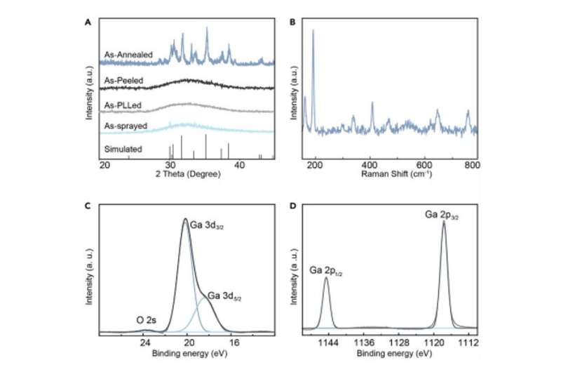 Structural analysis of liquid metal nano-patterns. (A) The crystallinity of the surface oxides of as-sprayed LMNPs, as-PLLed, as-peeled, and asannealed oxide package shells and simulated Ga2O3 XRD peaks. (B) Raman spectra of the annealed gallium oxide shell. (C and D) XPS curves of the Ga-O bonding. (C) XPS analysis indicating the energy peak of Ga 3d. (D) XPS analysis indicating the energy peak of Ga 2P. Credit: Matter (2022). DOI: 10.1016/j.matt.2022.01.004
Materials characterization and a breakthrough
The scientists confirmed the formation of laser-induced periodic liquid metal patterns via energy-dispersive X-ray spectroscopy methods and elemental mappings to show the presence of silicon, gallium and oxide, with liquid metal imprinted on the underlying substrate. The breakthrough laser technique also broke the laser optical limit. Licong An said, "Everyone knows that there is a direct correlation between the liquid metal pattern resolution and processing tool size, our breakthrough laser lithography broke this common knowledge, to generate patterns with sub-micron resolution for the first time."
He believes that "the patterns could reach a much higher calibration if a laser with a smaller wavelength is used." The team also simulated the formation of nanopatterns and emphasized the one-step process of direct liquid metal pattern deposition; another significant feature of the study. They combined a range of experimental methods to characterize the proprietary elemental composition of the oxide package shell covering the liquid metal nanopatterns with boosted mechanical properties—compared to pre-existing conventional methods of liquid-metal pattern generation.
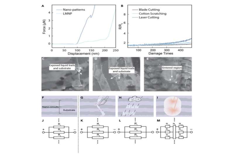 Mechanical and electrical properties of liquid metal nano-patterns. (A) Force-displacement curve of liquid metal nano-patterns and liquid metal particles. (B) Relative change in resistance (R/R0) as a function of the damage times. (C–E) Ruptured surface morphology after mechanical and thermal damage: (C), mechanical cutting; (D) mechanical scratching; (E), laser damage. Scale bar, 500 nm. (F–I) Schematics of the liquid metal nano-patterns without any damage (F), after mechanical cutting (G), after mechanical scratching (H), and after laser damage (I). (J–M) Schematic of electric response of liquid metal nano-patterns without any damage (J), after mechanical cutting (K), after mechanical scratching (L), and (M) after laser damage. Credit: Matter (2022). DOI: 10.1016/j.matt.2022.01.004
Outlook: Progress and potential
In this way, Licong An and colleagues developed electronically self-protective, high-resolution liquid metal patterns via a pulsed laser lithography (PLL) method to create one of the highest resolution liquid metal patterns to date. The team envision applications of the new material in next-generation nanoscale practices, with high integration densities, suited for demanding applications. The research team comprised of key collaborations between the primary author and Research Fellow Licong An, and interdisciplinary colleagues, including Professor Gary J. Cheng, a Fellow of the American Association for the Advancement of Science.
More information: Licong An et al, Self-packaged high-resolution liquid metal nano-patterns, Matter (2022). DOI: 10.1016/j.matt.2022.01.004
Bülent Öktem et al, Nonlinear laser lithography for indefinitely large-area nanostructuring with femtosecond pulses, Nature Photonics (2013). DOI: 10.1038/nphoton.2013.272
© 2022 Science X Network
Citation: Generating high-resolution self-packaged liquid metal nanopatterns (2022, May 23) retrieved 27 June 2022 from https://phys.org/news/2022-05-high-resolution-self-packaged-liquid-metal-nanopatterns.html
This document is subject to copyright. Apart from any fair dealing for the purpose of private study or research, no part may be reproduced without the written permission. The content is provided for information purposes only.
