Nov 07, 2022
(Nanowerk News) In recent years, global digitalization has seen unprecedented acceleration. Video streaming and video conferencing in home office and remote learning settings has resulted in a spike in residential broadband usage. Emerging applications such as artificial intelligence and autonomous vehicles will further accelerate the need for data communication in the future. Today’s internet infrastructure is built on fiber-optic communications, but how can the fiber-optic communication systems be made more efficient to fulfill future digital communication needs?
To cope with the increasing data rates, fiber-optic communication systems use many individual communication channels at dedicated wavelengths, a technique known as wavelength division multiplexing. The channels are combined in a multiplexer before transmission over an optical fiber. To retrieve the data, the optical spectrum is de-multiplexed on the receiver side. Commonly, this operation is performed using photonic integrated circuits (PICs). PICs confine and guide light into microscale components that manipulate information in multiple wavelength channels, such as arrayed waveguide gratings or integrated ring resonators.
In a paper published in the Journal of Optical Microsystems ("Silicon photonic microelectromechanical systems add-drop ring resonator in a foundry process"), Hamed Sattari and co-authors have now demonstrated a power-efficient component for the demultiplexing operation by physically moving a suspended silicon ring resonator in a photonic integrated circuit.
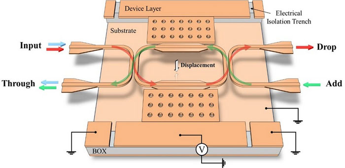
 Schematic representation of the MEMS add-drop filter. The device is tuned by actuating the vertically movable suspended ring resonator. The extremely compact footprint allows fast operation, and the electrostatic actuation mechanism ensures an extremely low power consumption, which makes this new filter highly energy efficient. (Image courtesy of the researchers)
The mechanical displacement of the ring resonator allows the extraction of a wavelength channel into a bus waveguide, effectively acting as a micro-mechanically operated add-drop filter. The electrostatic actuation mechanism builds on micro-electro-mechanical systems (MEMS), a technology widely implemented in consumer electronics, such as micromirrors for video projectors.
Compared to these established optical MEMS, the novel silicon photonic MEMS demonstrated in the paper is about 3 orders of magnitude smaller. The waveguide cross-section of the ring resonator is less than 650 nm x 220 nm, and a displacement of less than 500 nm is sufficient to operate the filter. This compact footprint allows fast operation compared to established MEMS products, and the electrostatic actuation mechanism ensures an extremely low power consumption, making this new filter highly energy efficient.
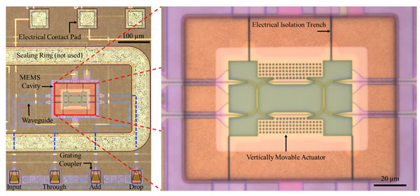
 Optical microscope image of the silicon photonic chip area in the left and a closer view of the suspended MEMS micro-ring resonator filter in the right. Successful integration of the MEMS device in the full stack of standard silicon photonic platform next to the grating couplers and the electrical bond pads. (Image courtesy of the researchers)
The silicon photonic MEMS add-drop filter has been implemented by postprocessing on a standard silicon photonics platform from IMEC, an international research and development organization with headquarters in Belgium. “The integration of MEMS in silicon photonics that has been manufactured in a standardized foundry process represents a technology milestone. We demonstrate that photonic MEMS can be integrated alongside established high-performance photonic components on-chip and can be scaled to large volumes” said Niels Quack, who led photonic MEMS development activity at EPFL, Switzerland (now at the University of Sydney).
“Our contribution demonstrates that silicon photonic MEMS have taken an important step forward in technology maturity,” said Sattari. “Large-scale photonic integrated circuits composed of thousands of components such as the add-drop filter can now be built, providing a missing platform that can make data-center and fiber-optic communication applications more energy efficient.”
The work was performed in the framework of the European project MORPHIC.
Source: International Society for Optics and Photonics
Share this:
 Schematic representation of the MEMS add-drop filter. The device is tuned by actuating the vertically movable suspended ring resonator. The extremely compact footprint allows fast operation, and the electrostatic actuation mechanism ensures an extremely low power consumption, which makes this new filter highly energy efficient. (Image courtesy of the researchers)
The mechanical displacement of the ring resonator allows the extraction of a wavelength channel into a bus waveguide, effectively acting as a micro-mechanically operated add-drop filter. The electrostatic actuation mechanism builds on micro-electro-mechanical systems (MEMS), a technology widely implemented in consumer electronics, such as micromirrors for video projectors.
Compared to these established optical MEMS, the novel silicon photonic MEMS demonstrated in the paper is about 3 orders of magnitude smaller. The waveguide cross-section of the ring resonator is less than 650 nm x 220 nm, and a displacement of less than 500 nm is sufficient to operate the filter. This compact footprint allows fast operation compared to established MEMS products, and the electrostatic actuation mechanism ensures an extremely low power consumption, making this new filter highly energy efficient.
 Optical microscope image of the silicon photonic chip area in the left and a closer view of the suspended MEMS micro-ring resonator filter in the right. Successful integration of the MEMS device in the full stack of standard silicon photonic platform next to the grating couplers and the electrical bond pads. (Image courtesy of the researchers)
The silicon photonic MEMS add-drop filter has been implemented by postprocessing on a standard silicon photonics platform from IMEC, an international research and development organization with headquarters in Belgium. “The integration of MEMS in silicon photonics that has been manufactured in a standardized foundry process represents a technology milestone. We demonstrate that photonic MEMS can be integrated alongside established high-performance photonic components on-chip and can be scaled to large volumes” said Niels Quack, who led photonic MEMS development activity at EPFL, Switzerland (now at the University of Sydney).
“Our contribution demonstrates that silicon photonic MEMS have taken an important step forward in technology maturity,” said Sattari. “Large-scale photonic integrated circuits composed of thousands of components such as the add-drop filter can now be built, providing a missing platform that can make data-center and fiber-optic communication applications more energy efficient.”
The work was performed in the framework of the European project MORPHIC.
Source: International Society for Optics and Photonics
Share this:
Nanowerk Newsletter
Get our daily Nanotechnology News to your inbox!

