Nov 07, 2022
(Nanowerk News) There is a long-standing folk art in China called "rice carving", which is to carve lifelike artistic patterns on rice with a length of only about 5 mm, which need to be appreciated with a magnifying glass, as shown in Figure 1.
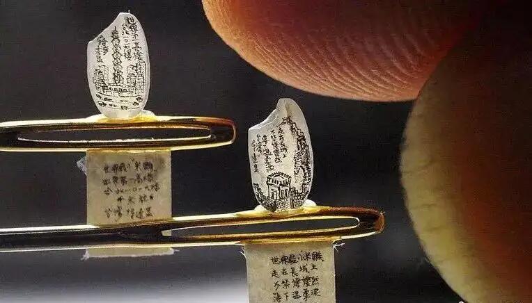 Figure 1. Rice sculpture.
Rice carving can be regarded as a printing technology based on a special material. Printing technology refers to the whole process of transferring images and information to the surface of paper, textiles, plastics and other materials. It is an important part of the information industry.
As an energy-saving, environment-friendly and difficult to copy printing method, ink-free color printing is becoming a new direction of printing technology development. The ink-free color printing uses laser engraving, holographic technology, electron beam, ultra-precision numerical control processing, electrochemical and other micro processing technologies to form digitally programmed micro-nano structures on the surface of printed products. Thereby, ink-free color printing can generate physical phenomena such as diffraction, reflection, refraction and transmission of light, and thus displaying characters and images of different colors.
The complex micro structure manufacturing process makes it difficult to be copied. Therefore, ink-free printing technology is widely used in packaging, labeling, anti-counterfeiting and other fields, and has the characteristics of ultra-high resolution and can display micron level characters.
However, due to the limitation of its simple light field manipulation principle, ink-free printing technology is difficult to produce more abundant colors and complex image information, and it has encountered great technical obstacles in its deep application. It can be expected that it will be difficult to make major breakthroughs in the future.
Therefore, the related fields are very eager for a full-color, continuous grayscale, high-resolution and simple structure color ink-free printing refresh technology, so as to play a key role in key fields such as optical encryption and anti-counterfeiting, AR / VR, printing and packaging, art creation, information storage and so on.
Metasurface is a type of artificial structure material developed rapidly in recent years. It is composed of periodic subwavelength structures deposited on planar substrates. In the optical band, by reasonably designing the geometry, size and orientation of the sub-wavelength structure, metasurface can flexibly manipulate the basic optical parameters such as amplitude, phase and polarization state of incident light at the nanoscale. It is the preferred technology for storing and displaying nanoprinting images with ultra-high resolution.
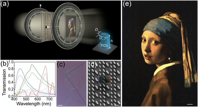 Figure 2. Left: Schematic for generating a full-color nanopainting image. Insets show a constituent titanium dioxide nanopillar and a scanning electron microscope image of the fabricated nanopillars. False color shading indicates the primary colors generated by the nanopillars. Scale bar: 500 nm. Right: Experimental color image of “Girl With a Pearl Earring” generated under white-light illumination. Scale bar: 50 µm (Image: T. Xu/Nanjing University)
As a new type of optical image storage and display platform based on metasurfaces, the resolution of the stored image is as high as 80K DPI, which not only far exceeds the traditional printing technology (such as gravure printing, which is generally only 5K DPI), but also has the outstanding characteristics of long life, zero pollution and rich color.
Fig. 2 shows the results of recording and reproducing the "girl with pearl earrings" artwork with a metasurface with an overall size of about 0.6 mm x 1 mm (read more: "Photorealistic nanopainting with light").
More importantly, the rich design freedom of metasurfaces has made the metasurface-based nanoprinting technology develop from the original single-channel to current multi-channel, multi-function integration and even dynamic display, showing attractive application prospects in the fields of information storage, optical anti-counterfeiting, information encryption and ultra-compact display, as shown in Fig. 3.
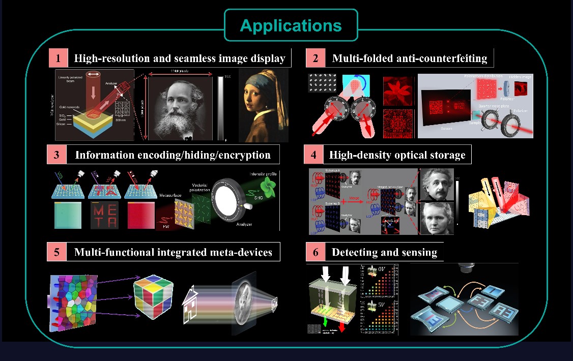 Figure 3. Applications of metasurface-based nanoprinting.
The authors of this article (Opto-Electronic Advances, "Metasurface-based nanoprinting: principle, design and advances") summarize the development of metasurface-based nanoprinting in recent years. Based on the physical principle of metasurface-based nanoprinting, this paper reviews in detail the research progress of single-channel metasurface-based nanoprinting, multi-channel metasurface-based nanoprinting, dynamic metasurface-based nanoprinting and multi-functional metasurfaces combining nanoprinting with holography or metalens.
The authors also discuss the applications of metasurface-based nanoprinting in image display, vortex beam generation, information decoding and hiding, information encryption, high-density optical storage and optical anti-counterfeiting, and finally summarizes the opportunities and challenges that metasurface-based nanoprinting currently faces.
Source: Compuscript
Share this:
 Figure 1. Rice sculpture.
Rice carving can be regarded as a printing technology based on a special material. Printing technology refers to the whole process of transferring images and information to the surface of paper, textiles, plastics and other materials. It is an important part of the information industry.
As an energy-saving, environment-friendly and difficult to copy printing method, ink-free color printing is becoming a new direction of printing technology development. The ink-free color printing uses laser engraving, holographic technology, electron beam, ultra-precision numerical control processing, electrochemical and other micro processing technologies to form digitally programmed micro-nano structures on the surface of printed products. Thereby, ink-free color printing can generate physical phenomena such as diffraction, reflection, refraction and transmission of light, and thus displaying characters and images of different colors.
The complex micro structure manufacturing process makes it difficult to be copied. Therefore, ink-free printing technology is widely used in packaging, labeling, anti-counterfeiting and other fields, and has the characteristics of ultra-high resolution and can display micron level characters.
However, due to the limitation of its simple light field manipulation principle, ink-free printing technology is difficult to produce more abundant colors and complex image information, and it has encountered great technical obstacles in its deep application. It can be expected that it will be difficult to make major breakthroughs in the future.
Therefore, the related fields are very eager for a full-color, continuous grayscale, high-resolution and simple structure color ink-free printing refresh technology, so as to play a key role in key fields such as optical encryption and anti-counterfeiting, AR / VR, printing and packaging, art creation, information storage and so on.
Metasurface is a type of artificial structure material developed rapidly in recent years. It is composed of periodic subwavelength structures deposited on planar substrates. In the optical band, by reasonably designing the geometry, size and orientation of the sub-wavelength structure, metasurface can flexibly manipulate the basic optical parameters such as amplitude, phase and polarization state of incident light at the nanoscale. It is the preferred technology for storing and displaying nanoprinting images with ultra-high resolution.
 Figure 2. Left: Schematic for generating a full-color nanopainting image. Insets show a constituent titanium dioxide nanopillar and a scanning electron microscope image of the fabricated nanopillars. False color shading indicates the primary colors generated by the nanopillars. Scale bar: 500 nm. Right: Experimental color image of “Girl With a Pearl Earring” generated under white-light illumination. Scale bar: 50 µm (Image: T. Xu/Nanjing University)
As a new type of optical image storage and display platform based on metasurfaces, the resolution of the stored image is as high as 80K DPI, which not only far exceeds the traditional printing technology (such as gravure printing, which is generally only 5K DPI), but also has the outstanding characteristics of long life, zero pollution and rich color.
Fig. 2 shows the results of recording and reproducing the "girl with pearl earrings" artwork with a metasurface with an overall size of about 0.6 mm x 1 mm (read more: "Photorealistic nanopainting with light").
More importantly, the rich design freedom of metasurfaces has made the metasurface-based nanoprinting technology develop from the original single-channel to current multi-channel, multi-function integration and even dynamic display, showing attractive application prospects in the fields of information storage, optical anti-counterfeiting, information encryption and ultra-compact display, as shown in Fig. 3.
 Figure 3. Applications of metasurface-based nanoprinting.
The authors of this article (Opto-Electronic Advances, "Metasurface-based nanoprinting: principle, design and advances") summarize the development of metasurface-based nanoprinting in recent years. Based on the physical principle of metasurface-based nanoprinting, this paper reviews in detail the research progress of single-channel metasurface-based nanoprinting, multi-channel metasurface-based nanoprinting, dynamic metasurface-based nanoprinting and multi-functional metasurfaces combining nanoprinting with holography or metalens.
The authors also discuss the applications of metasurface-based nanoprinting in image display, vortex beam generation, information decoding and hiding, information encryption, high-density optical storage and optical anti-counterfeiting, and finally summarizes the opportunities and challenges that metasurface-based nanoprinting currently faces.
Source: Compuscript
Share this:
Nanowerk Newsletter
Get our daily Nanotechnology News to your inbox!

