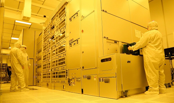
 Cleanroom technicians at the AIM Photonics NanoTech chip fabrication facility in Albany, N.Y. Courtesy of SUNY Polytechnic Institute.
AIM Photonics will incorporate these calibration structures into its process design kit (PDK) used by engineers when designing new chips for fabrication at AIM’s facilities.
Cleanroom technicians at the AIM Photonics NanoTech chip fabrication facility in Albany, N.Y. Courtesy of SUNY Polytechnic Institute.
AIM Photonics will incorporate these calibration structures into its process design kit (PDK) used by engineers when designing new chips for fabrication at AIM’s facilities.
Experts from both organizations are already working to integrate the new measurement structures into AIM Photonics’ foundry process, NIST said. An updated PDK with the calibration structures is expected to be available in approximately one year.
“This effort will leverage NIST’s expertise in chip measurements, calibration, and integrated device modeling,” said Under Secretary of Commerce for Standards and Technology and NIST Director Laurie E. Locascio. Though planning for this effort began before the passage of the CHIPS Act, it aligns with the act’s goals. “This shows how government and industry can work together to drive innovation and restore U.S. global leadership in semiconductor manufacturing.”
Earlier this year, supported by American Rescue Act funding, NIST earmarked over $5 million for AIM’s development of photonic technologies addressing the pandemic. The majority of the $5 million was targeted for AIM’s development of disposable integrated photonics-based tests.
