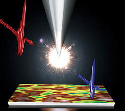
MAPbI3 is of interest as a material that could potentially replace silicon in solar cells.
THz light from the newly introduced probe scanning microscope is shined through a sharp, metallic tip that enhances the microscope’s capabilities to image at nanometer-length scales. “Normally if you have a lightwave, you cannot see things smaller than the wavelength of the light you’re using,” researcher Richard Kim said. “For this terahertz light, the wavelength is about a millimeter, so it’s quite large. But here we used this sharp metallic tip with an apex that is sharpened to a 20-nm radius curvature, and this acts as our antenna to see things smaller than the wavelength that we were using.”

Instead, they observed significant variation in light scattering along the grain boundaries in the perovskite. This observation gave the researchers insight into the material’s degradation issues.
When the researchers applied THz near-field nanoconductivity mapping to the perovskite, they found that the perovskite showed distinct dielectric heterogeneity, due to charge trapping and degradation at the single-grain boundary level. The researchers extracted a quantitative profile of trapping density in the vicinity of the grain boundaries with sub-20-nm resolution.
Over the course of a week, as the team collected data on the material, the researchers tracked the degradation process through changes in the levels of light scattering. Tracking local nanodefect distributions in the material over time allowed the researchers to identify a distinct degradation pathway in the material that started from the grain boundaries and propagated inside the grains over time.
The researchers said that the direct visualization and quantitative evaluation of charge filling in grain boundary traps of hybrid metal halide perovskites require dynamic conductivity imaging simultaneously at the THz wavelength and nanometer scale. This capability, they said, is not provided by conventional transport and imaging methods.
“We believe that the present study demonstrates a powerful microscopy tool to visualize, understand, and potentially mitigate grain boundary degradation, defect traps, and materials degradation,” researcher Jigang Wang said. “Better understanding of these issues may enable developing highly efficient perovskite-based photovoltaic devices for many years to come.”
The primary challenge to using MAPbI3 perovskite in solar cells is that it degrades easily when exposed to elements like heat and moisture. The information obtained through the Ames study could be used to manipulate and further develop the material to improve its reliability.
The single-grain boundary, nano-THz conductivity imaging demonstrated by the researchers could be extended to benchmark various perovskite materials and devices for their global photoenergy conversion performance and local charge transfer proprieties of absorbers and interfaces.
The research was published in ACS Photonics (www.pubs.acs.org/doi/10.1021/acsphotonics.2c00861).

