The photomemristor is based on 2D graphene/MoS2-xOx/graphene (G/M/G) structures. Photoexcited carriers and oxygen-related ions are coupled in the two-terminal G/M/G architecture, leading to a displaced and pinched hysteresis in the device’s current-voltage characteristic (also known as I-V curve).
The nonvolatile photomemristor can store and read multiple photoresponse states in a nonvolatile mode at zero external voltage. Its switching properties can be jointly controlled by the electric-field-driven migration of ions and photo-induced redox reactions at the asymmetric G/M/G contacts.
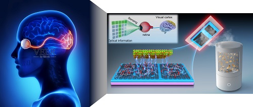
By mimicking the biological functions of the human retina and designing specific device structures, the researchers made it possible for the photomemristor to act as a neural network for neuromorphic visual processing and for the implementation of computationally complete photoresponse-stateful logic operations triggered by electrical and light stimuli together.
According to the researchers, the two-terminal photomemristor can support versatile sensing-memory-computing approaches for implementing an in-sensor computing network.
“We designed a two-terminal device with MoS2-xOx and specific graphene for three purposes in one,” the researchers said. “One — to provide low-barrier energy for the migration of oxygen ions; two — to perform as geometry-asymmetric, metal/semiconductor/metal van der Waals heterostructures with multiphotoresponse states; and three — as an extension of a memristor, this device not only provides tunable conductance, but also demonstrates reconfigurable photoresponse for reading at zero bias voltage.”
The researchers said that the tunable short-circuit photocurrent and photoresponse can be increased to 889.8 nA and 98.8 mA/W, respectively. This is a much higher value than other reconfigurable phototransistors based on 2D materials can achieve, the researchers added.
“To reverse the channel polarity and obtain a gate-tunable short-circuit photocurrent, the channel semiconductor must be thin enough. Thus, it is difficult to use the thick film needed to absorb enough light to get a large signal,” the researchers said. “In our case, the mechanism of the two-terminal device rearrangement is based on ion migration, which is not limited by the thickness. We can increase the thickness of the film to absorb more photons and get a large short-circuit photocurrent.
“This new concept of a two-terminal photomemristor not only enables all-in-one sensing-memory-computing approaches for neuromorphic vision hardware, but also brings great convenience for high-density integration.”