
| Date | 17th, Mar 2023 |
|---|
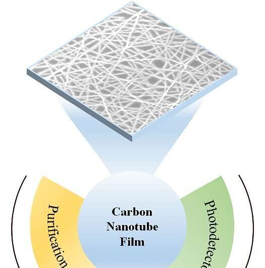
 With additional optimization and research, highly purified semiconducting single-walled carbon nanotube (s-SWCNT) films will exceed current photodetector performance and efficiency at a significantly lower cost. The technology will be integrated into a variety of different optoelectronic devices capable of detecting and processing light. Credit: Nano Research Energy
Semiconducting single-walled carbon nanotubes (s-SWCNTs) are being used to develop a third generation of optimized shortwave infrared photodetectors that will improve pixel size, weight, power consumption, performance and cost over photodetectors made from traditional materials.
Ultrasensitive shortwave infrared photodetectors, which detect a subset of shortwave infrared light wavelengths outside of the visual spectrum, have many potential applications, including night surveillance, navigation during poor weather conditions, fiber optic communications and semiconductor quality control.
Shortwave infrared photodetectors have traditionally been made out of III-V materials like indium gallium arsenide (InGaAs). InGaAs photodetectors are expensive, however, and current research into alternative photodetector materials, such as s-SWCNTs, will ideally reduce the cost of shortwave infrared photodetectors while increasing both performance and efficiency.
A team of leading scientists from Peking University outlined the current technology and challenges associated with developing s-SWCNT films into shortwave infrared photodetectors to spur additional research and applications of the technology. Current advances in solution purification technology will facilitate the development of high-purity s-SWCNT films suitable for large-area, homogenous and high-performance optoelectronic devices and applications that detect and process light, including photodetectors.
Further optimization of film purity, thickness, clarity and array alignment must be achieved before s-SWCNT films will meet or exceed the performance level of traditional, more expensive photodetectors made of InGaAs or similar materials.
The team published their review in the March 16 issue of Nano Research Energy.
"Reviewing the progress of the s-SWCNTs film photodetectors can clarify the current research status, challenges and applications of s-SWCNT film photodetectors and optoelectronic integration," said Sheng Wang, one of the authors of the review paper and associate professor at the School of Electronics at Peking University, China.
"We outlined s-SWCNT technology in three sections: (1) the current research status of the s-SWCNT film photodetectors, (2) the current research status of monolithic/three-dimension optoelectronic integration based on s-SWCNT film photodetectors and (3) the requirements of s-SWCNT film and device structure for ideal s-SWCNT film photodetectors and optoelectronic integration," said Wang.
"The next step in the field is to improve the performance of s-SWCNT film photodetectors by optimizing the s-SWCNT films and device structure. For the s-SWCNT film optimization, the semiconductor purity of a uniform s-SWCNT film needs to be greater than 99.9999%," said Wang.
Achieving these purity levels is not a trivial matter. Early purification methods attempted to burn off s-SWCNT impurities after films were grown but resulted in films with many defects. Since then, conjugated polymers have been used to purify s-SWCNTs not only from impurities, but also by their diameter, as different diameters of s-SWCNT determine which wavelengths the films can detect. Recently, a sorting process has achieved the s-SWCNT purity levels required for high-performance electronics.
Optimization is also required in s-SWCNT film preparation, including thickness, clarity and alignment. Many methods have been developed to grow s-SWCNT films, but deposition and dip-coating methods are often favored for their simplicity, stability and the homogenous films they produce. One scalable and efficient method of dip coating controls s-SWCNT deposition by simply modifying the number of times a substrate is lifted out of an organic solvent of dispersed s-SWCNTs and the speed of each lift.
The electronics field recognizes the potential of s-SWCNTs as a suitable material for high-performance shortwave infrared detectors, but a significant performance gap exists between traditional photodetectors, made of materials such as InGaAs, and s-SWCNT film photodetectors. "The ultimate goal is to optimize the performance of s-SWCNT film photodetectors, so they are comparable to commercial photodetectors at a lower cost," said Wang.
The researchers believe this increase in performance and decrease in cost will result in the integration of more shortwave infrared photodetector films into devices and the development of new optoelectronic applications in the future. The field also aspires to integrate high-performance carbon nanotubes in electric circuits.
More information: Xiang Cai et al, Recent progress of photodetector based on carbon nanotube film and application in optoelectronic integration, Nano Research Energy (2023). DOI: 10.26599/NRE.2023.9120058
Provided by Tsinghua University Press
Citation: Carbon nanotube films as ultrasensitive photodetectors: Progress and challenges (2023, March 17) retrieved 26 March 2023 from https://phys.org/news/2023-03-carbon-nanotube-ultrasensitive-photodetectors.html
This document is subject to copyright. Apart from any fair dealing for the purpose of private study or research, no part may be reproduced without the written permission. The content is provided for information purposes only.
